Conductive polymer electronic devices with surface mountable configuration and methods for manufacturing same

a technology of conductive polymer electronic components and configurations, applied in the direction of resistor details, conductive pattern formation, thick film resistors, etc., can solve the problems of metal elements imposing physical constraints, poor resistance stability of typical prior art conductive polymer ptc devices, and inability to manufactur

Active Publication Date: 2011-07-21
BOURNS INC
View PDF15 Cites 20 Cited by
  • Summary
  • Abstract
  • Description
  • Claims
  • Application Information

AI Technical Summary

Benefits of technology

[0014]In a still further embodiment, a surface-mountable conductive polymer electronic device comprises a conductive polymer active layer laminated between an upper electrode and a lower electrode; an upper insulation layer applied on the upper electrode and a lower insulation layer applied on the lower electrode; first and second planar conductive terminals formed on the lower insulation layer; a first cross-conductor connecting the lower electrode and the first terminal, and separated from the upper electrode by a portion of the upper insulation layer; and a second cross-conductor connecting the upper electrode and the second terminal, and separated from the lower electrode by a portion of the lower insulation layer. The invention also encompasses a multi-active layer device that comprises two or more single active layer devices, as defined above, arranged in a vertically-stacked configuration and electrically connected in parallel.

Problems solved by technology

One problem with surface-mountable conductive polymer devices is that the metal elements tend to impose a physical constraint on the thermal expansion of the polymeric element(s) when they experience an over-current situation.
To the extent that the metallic elements of such a device impose physical constraints on the expansion of the conductive polymer element(s), the functionality of the device may be impaired, especially after repeated over-current “trippings.” For example, “repeatability” (the characteristic of the device to exhibit substantially the same operational parameters) may degrade over a multitude of duty cycles (over-current tripping and subsequent resetting upon removal of the overvoltage), due to a kind of stress-induced “hysteresis” effect.
In particular, typical prior art conductive polymer PTC devices tend to exhibit poor resistance stability as a function of the number of duty cycles.
Furthermore, to the extent that the metal elements allow at least some degree of polymeric expansion, the metal elements are subject to mechanical stresses that may compromise the physical integrity of the device over repeated duty cycles.
Thus, there has been a long-felt, but as yet unsatisfied, need for a surface-mountable conductive polymer resistive device, particularly a PTC device, that is economical to manufacture, that has a small circuit board footprint, and that allows adequate thermal expansion of the polymer element without subjecting the metal elements to undue stress.

Method used


Image

  • Conductive polymer electronic devices with surface mountable configuration and methods for manufacturing same
  • Conductive polymer electronic devices with surface mountable configuration and methods for manufacturing same
  • Conductive polymer electronic devices with surface mountable configuration and methods for manufacturing same

Examples


first embodiment

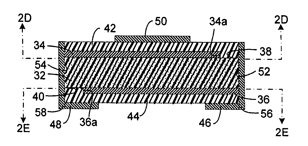
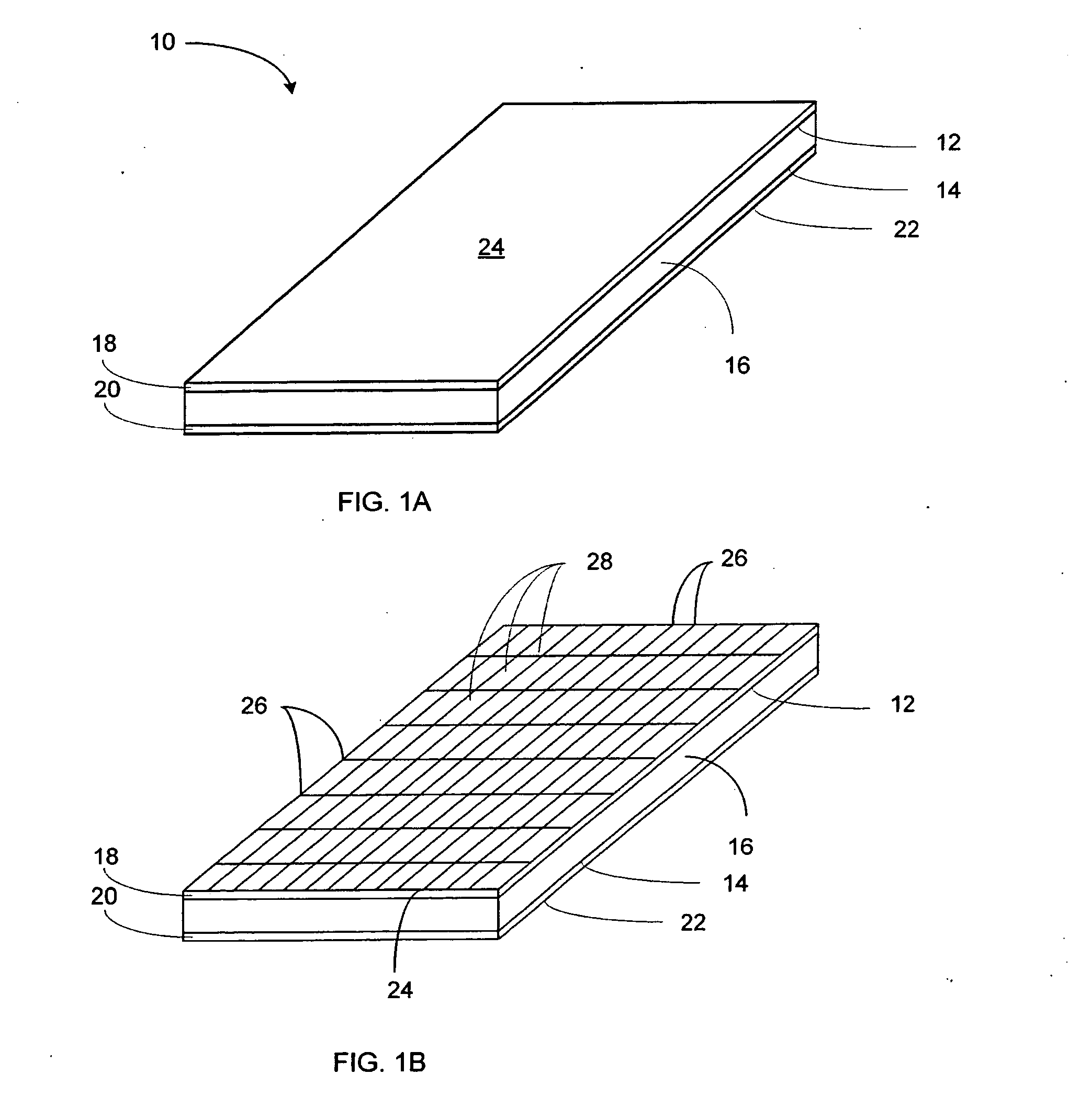
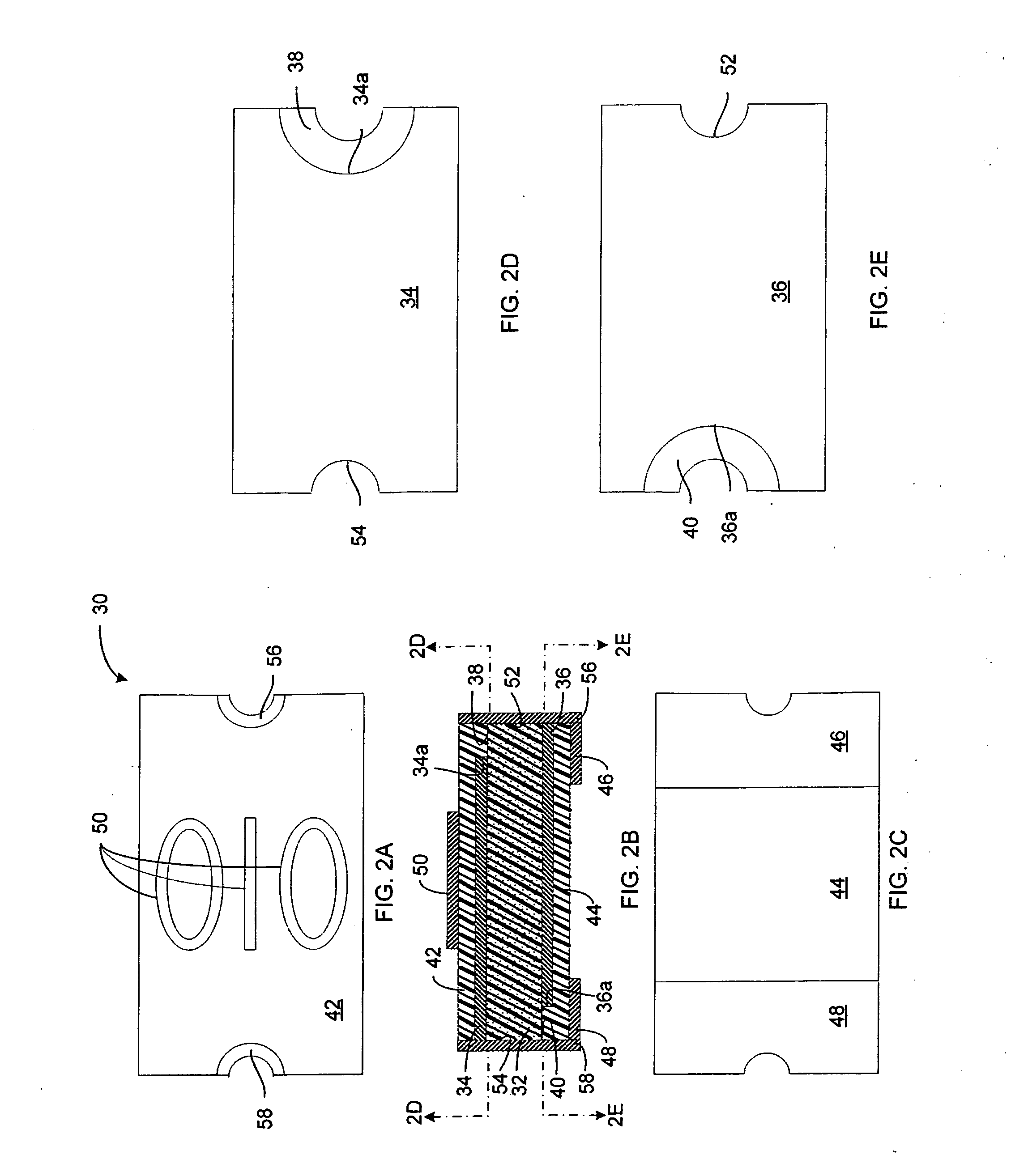
[0053]FIGS. 2A, 2B, 2C, 2D, and 2E illustrate a conductive polymer device 30, in accordance with the present invention. The device 30 includes a single active layer 32 of conductive polymer material, laminated between an upper metal foil electrode 34 and a lower foil electrode 36. First and second pluralities of through-hole via locations are defined in the sheet structure 10 (FIG. 1A). Each via location in the first plurality is separated from a corresponding via location in the second plurality by a pre-defined distance that corresponds to the length of a single device 30. An arcuate area of the upper electrode 34 adjacent each of the first via locations is removed (e.g. by conventional photo-resist masking and etching) to create an upper isolation area 38 at a first end of the upper electrode 34. Similarly, an arcuate area of the lower electrode 36 adjacent each of the second via locations is removed to create a lower isolation area 40 at the opposite end of the second electrode ...

second embodiment

[0062]FIGS. 4A, 4B, and 4C illustrate a conductive polymer device 130, in accordance with the invention. The device 130 includes a single active layer 132 of conductive polymer material, laminated between an upper metal foil electrode 134 and a lower foil electrode 136. The device 130 is similar to the device 30, described above and illustrated in FIGS. 2A through, 2E, except that the upper electrode 134 is formed (by photo-resist masking and etching) with an upper isolation area 138 in the form of a narrow lateral band or strip that is spaced from a first end of the device 130 by a narrow upper residual foil area 139. Similarly, the lower electrode 136 is likewise formed with a lower isolation area 140 in the form of a narrow lateral band or strip that is spaced from the second end of the device 130 by a narrow lower residual foil area 141. A top insulation layer 142 is applied or formed over the upper electrode 134 and the upper residual foil area 139, filling in the upper isolati...

third embodiment

[0073]FIGS. 7A, 7B, and 7C illustrate a multiple active layer device 270 that is a variant of FIGS. 6A-6C, wherein the multiple active layer device 270 comprises at least a first active layer 272a and a second active layer 272b, of conductive polymer material, connected in parallel, and arranged in a vertically-stacked configuration with only a single pair of surface-mount terminals. The first active layer 272a is laminated between first and second metal foil electrodes 274a, 274b in a first laminated sheet structure, and the second active layer 276b is laminated between fifth and fourth metal foil electrodes 274c, 274d in a second laminated sheet structure, each of the sheet structures being of the type described above and shown in FIGS. 1A and 1B. The first and second pluralities of via locations are defined as described above. The first or upper electrode 274a is formed (by photo-resist masking and etching) with an arcuate upper isolation area 276a between the first electrode 274...


PUM

PropertyMeasurementUnit
thicknessaaaaaaaaaa
thicknessaaaaaaaaaa
thicknessaaaaaaaaaa

Abstract

Surface-mountable conductive polymer electronic devices include at least one conductive polymer active layer laminated between upper and lower electrodes. Upper and lower insulation layers, respectively, sandwich the upper and lower electrodes. First and second planar conductive terminals are formed on the lower insulation layer. First and second cross-conductors are provided by plated through-hole vias, whereby the cross-conductors connect each of the electrodes to one of the terminals. Certain embodiments include two or more active layers, arranged in a vertically-stacked configuration and electrically connected by the cross-conductors and electrodes in parallel. Several embodiments include at least one cross-conductor having a chamfered or beveled entry hole through the upper insulation layer to provide enhanced adhesion between the cross-conductor and the insulation layer. Several methods for manufacturing the present surface-mountable conductive polymer electronic devices are also provided.

Description

CROSS REFERENCE TO RELATED APPLICATIONS[0001]This application claims the benefit, under 35 U.S.C. §119(e), of co-pending Provisional Application No. 60 / 744,897, filed on Apr. 14, 2006, the disclosure of which is incorporated herein by reference.FEDERALLY SPONSORED RESEARCH OR DEVELOPMENT[0002]Not ApplicableBACKGROUND OF THE INVENTION[0003]This disclosure relates to the field of conductive polymer electronic components and devices. In particular, it relates to resistive devices comprising a layer of thermally-sensitive resistive material, such as a conductive polymer, that is laminated between a pair of planar electrodes, wherein the device has a surface-mountable configuration.[0004]Conductive polymer thermally-sensitive resistive devices have become commonplace on electronic circuits. These include devices that exhibit a positive temperature coefficient of resistivity (PTC) and a negative temperature coefficient of resistivity (NTC). In particular, resistive devices comprising a co...

Claims


Application Information

Patent Timeline
Patent Type & Authority Applications(United States)
IPC IPC(8): H01C7/13H05K3/10
CPCH01C1/1406H01C1/1413H01C7/005H01C1/016H01C7/021Y10T29/49165H01C7/041H01C7/049H01C7/18H01C17/02H01C7/028H01C17/281
Inventor BOURNS, GORDON L.CHU, STELARGRINDELL, DANIEL E.HUANG, DAVIDKELLY, JOHNMEIJER, ERIC
Owner BOURNS INC
Why Eureka
Try Eureka