Electromagnetic interference shield with integrated heat sink

a technology of electromagnetic interference shielding and heat sink, which is applied in the direction of lighting and heating apparatus, electrical apparatus casings/cabinets/drawers, instruments, etc., can solve the problems of cost and efficiency, ic packages that require both heat sinks and emi shielding, and the geometry of packages creates additional complexity

Active Publication Date: 2011-07-21
AVAGO TECH INT SALES PTE LTD
View PDF22 Cites 81 Cited by
  • Summary
  • Abstract
  • Description
  • Claims
  • Application Information

AI Technical Summary

Benefits of technology

Methods, systems, and apparatuses are described for EMI shields and heat sink lids for IC packages substantially as s...

Problems solved by technology

The dies in IC packages typically generate a great amount of heat during operation.
However, in many cases, the package geometry creates additional complexities in the mounting of such heat sinks.
As such, some IC packages need electromagnetic interference (EMI) shielding.
Conventional electronics system designs that require both heat sink and EMI shielding have problems with cost and efficiency.
From a thermal perspective this may be an acceptable...

Method used


Image

  • Electromagnetic interference shield with integrated heat sink
  • Electromagnetic interference shield with integrated heat sink
  • Electromagnetic interference shield with integrated heat sink

Examples


example emi

Shield Ring and Heat Sink Lid Embodiments

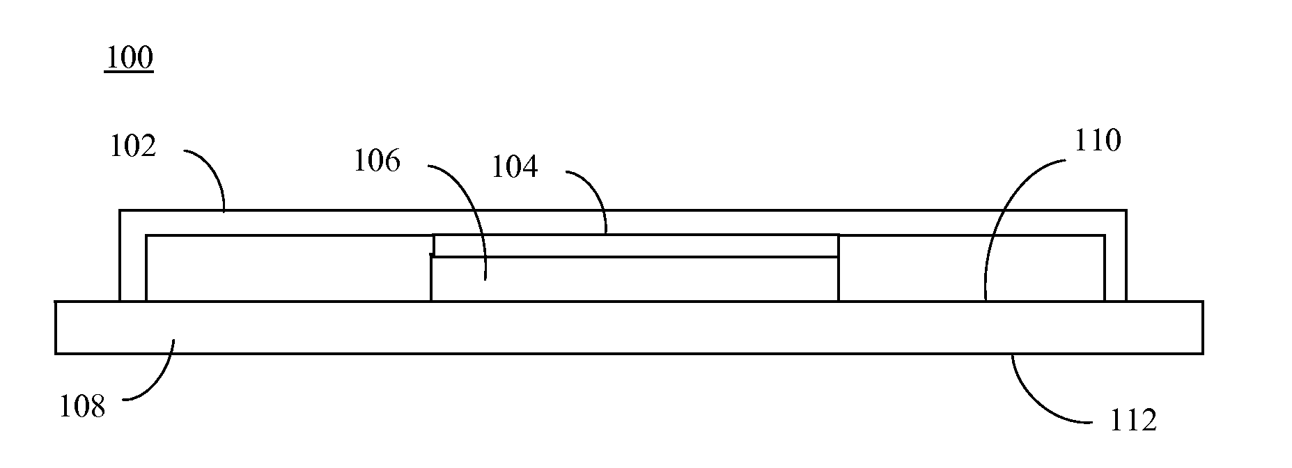
As described above, some electronic devices may be configured with a mechanical enclosure / shield that surrounds the electronic device to prevent tampering and to provide EMI shielding. For instance, the EMI shielding may protect the electronic device from receiving electromagnetic radiation and / or may block emitted electromagnetic radiation from the electronic device. However, the presence of the enclosure limits the thermal solutions that are available for such devices because an external heat sink cannot be mounted without (1) substantially increasing the height and cost of the shield by mounting the heat sink under the shield, or (2) substantially decreasing the efficiency of the heat sink by mounting the heat sink above the shield. With the continuous increase of power density in electronic components, there exists serious thermal challenges that are not solely addressed by IC package selection and design.

For example, FIG. 1 shows a cross...

example fabrication embodiments

Heat sink lids may be formed in a variety of ways, according to embodiments. For example, FIG. 28 shows a block diagram of a system 2800 for forming heat sink lids having a “bridged” form. For instance, heat sink lid 504 of FIG. 5 may be formed according to system 2800. As shown in FIG. 28, system 2800 includes an extrusion press 2802 and a cross-cutter 2804. Furthermore, extrusion press 2802 includes an extrusion die 2806. System 2800 is described as follows with respect to a flowchart 2900 shown in FIG. 29. Flowchart 2900 provides a process for forming heat sink lids, according to an example embodiment. Flowchart 2900 is described as follows.

As shown in FIG. 29, flowchart 2900 begins with step 2902. In step 2902, a stock material is extruded to form a heat sink lid strip having a cross-section defined by a die. For example, with reference to FIG. 28, extrusion press 2802 receives a stock material 2808. Stock material 2808 may be any suitable material for heat sink lids, including ...


PUM

PropertyMeasurementUnit
Temperatureaaaaaaaaaa

Abstract

A printed circuit board (PCB) assembly is provided that includes a PCB, an integrated circuit package, an electromagnetic interference (EMI) shield ring, and a heat sink lid. A first surface of the package is mounted to a first surface of the PCB. The EMI shield ring is mounted to the first surface of the PCB in a ring around the package. A first surface of the heat sink lid includes a recessed region and first and second supporting portions separated by the recessed region. The heat sink lid is mated with the EMI shield ring such that the package is positioned in an enclosure formed by the EMI shield ring and the recessed region of the heat sink lid. A second surface of the package may interface with a surface of the recessed region.

Description

BACKGROUND OF THE INVENTION1. Field of the InventionThe present invention relates to integrated circuit packaging technology.2. Background ArtA printed circuit board (PCB), also referred to as printed wiring board (PWB), is used to mechanically support and electrically connect electronic components mounted to the PCB. A PCB includes a stack of conductive and non-conductive layers attached together (e.g., laminated together). Conductive pathways (e.g., traces) are formed in the conductive layers (e.g., by etching) that are used to electrically connect the mounted electronic components.Examples of electronic components that may be mounted to PCBs are integrated circuit (IC) packages. IC packages typically include one or more chips / dies (e.g., from semiconductor wafers), and are used to environmentally protect the dies and to interface the dies to PCBs. IC packages may be configured in various ways to be mounted to a PCB, including having arrangements of pins, pads, solder balls, etc.,...

Claims


Application Information

Patent Timeline
IPC IPC(8): H05K7/20H05K3/10
CPCH01L21/4878Y10T29/49128H01L23/4093H01L23/552H05K1/0203H05K1/0218H05K9/0022H05K2201/10371H01L23/3675H01L2224/73253H01L2224/73204H01L2224/32225H01L2224/16225H01L2924/00
Inventor ZHAO, SAM ZIQUNWONG, CALVIN
Owner AVAGO TECH INT SALES PTE LTD
Why Eureka
Try Eureka