Switchable Neutral Beam Source

a neutral beam source and switchable technology, applied in the field of substrate processing, can solve the problems of electrically charged particles, tolerance of semiconductor structures, manufacturing of semiconductor devices, etc., and achieve the effect of reducing the roughness of the line edg

Inactive Publication Date: 2011-07-21
TOKYO ELECTRON LTD
View PDF24 Cites 52 Cited by
  • Summary
  • Abstract
  • Description
  • Claims
  • Application Information

AI Technical Summary

Benefits of technology

[0016]The invention can provide apparatus and methods of processing a substrate in real-time using subsystems and processing sequences created to modify radiation-sensitive materials. In addition, the modified radiation-sensitive lay

Problems solved by technology

However, the use of plasma (i.e., electrically charged particles), itself, produces problems in the manufacture of semiconductor devices.
Therefore, the tolerance of semiconductor structures for the charge carried by particles impinging on them during the manufacturing process, such as a dry plasma etching process, has become quite limited and the structures for

Method used


Image

  • Switchable Neutral Beam Source
  • Switchable Neutral Beam Source
  • Switchable Neutral Beam Source

Examples


Embodiment Construction

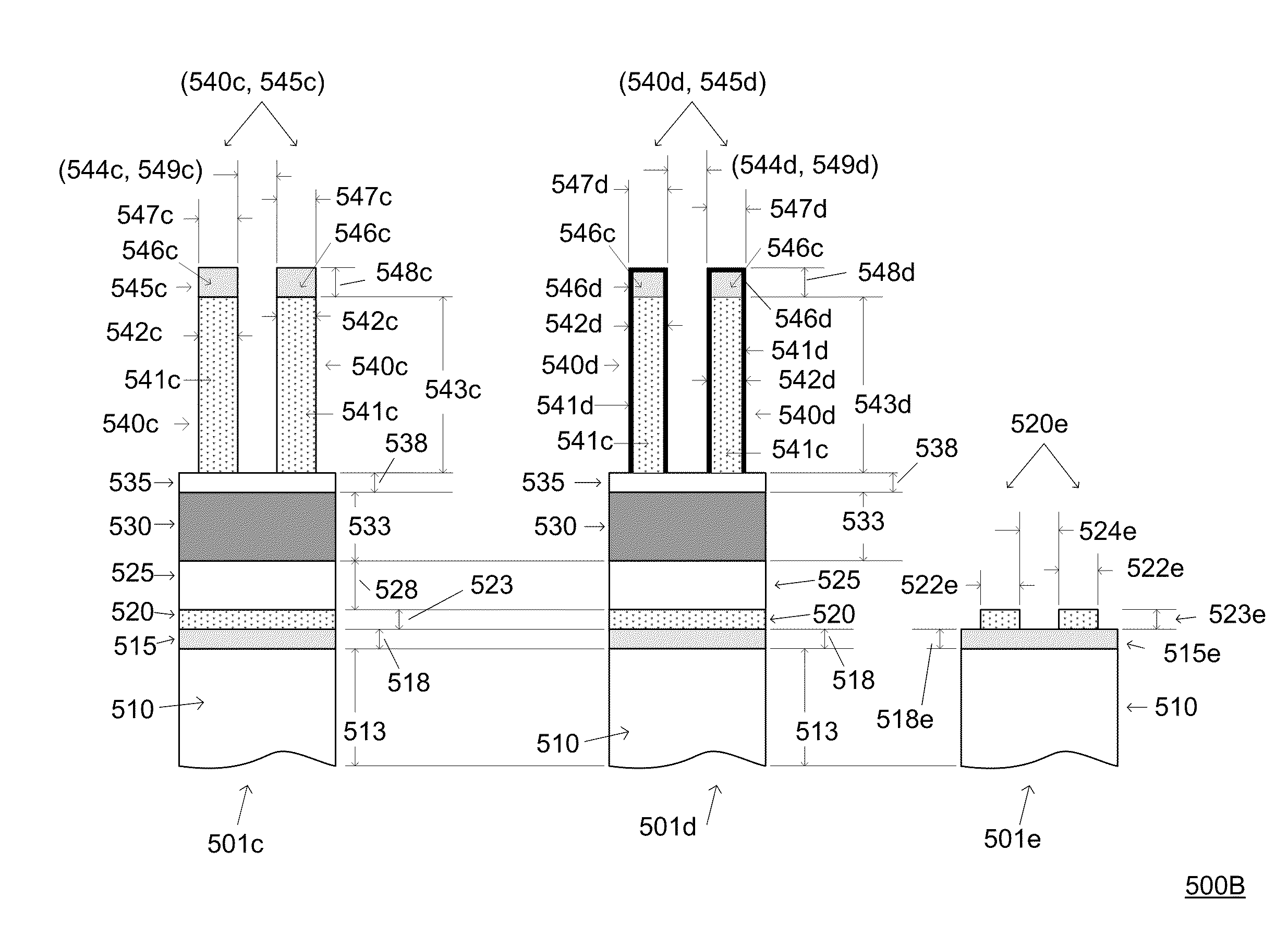
[0025]The invention provides apparatus and methods of processing a substrate in real-time using switchable quasi-neutral beam (SQNB) subsystems and SQNB processing sequences created to modify radiation-sensitive materials. In addition, the modified radiation-sensitive layer can be used to more accurately control gate and / or spacer critical dimensions (CDs), to control gate and / or spacer CD uniformity, and to eliminate line edge roughness (LER) and line width roughness (LWR). For example, the SQNB subsystems and SQNB processing sequences can be used to alter the mechanical properties of the masking layer materials, can be used to modify the chemical and / or mechanical properties of the masking layer materials, and can be used to alter the etch resistance of the masking layer materials.

[0026]In some embodiments, apparatus and methods are provided for creating and / or using a metrology library that includes profile data and diffraction signal data for modified photoresist features and pe...


PUM

PropertyMeasurementUnit
Temperatureaaaaaaaaaa
Timeaaaaaaaaaa

Abstract

The invention can provide apparatus and methods of processing a substrate in real-time using a switchable quasi-neutral beam system to improve the etch resistance of photoresist layer. In addition, the improved photoresist layer can be used in an etch procedure to more accurately control gate and/or spacer critical dimensions (CDs), to control gate and/or spacer CD uniformity, and to eliminate line edge roughness (LER) and line width roughness (LWR).

Description

BACKGROUND OF THE INVENTION[0001]1. Field of the Invention[0002]The present invention relates to substrate processing, and more particularly to improving the substrate processing using a switchable neutral beam source.[0003]2. Description of the Related Art[0004]During semiconductor processing, plasma is often utilized to assist etch processes by facilitating the anisotropic removal of material along fine lines or within vias (or contacts) patterned on a semiconductor substrate. Furthermore, plasma is utilized to enhance the deposition of thin films by providing improved mobility of adatoms on a semiconductor substrate.[0005]Once the plasma is formed, selected surfaces of the substrate are etched by the plasma. The process is adjusted to achieve appropriate conditions, including an appropriate concentration of desirable reactant and ion populations to etch various features (e.g., trenches, vias, contacts, etc.) in the selected regions of the substrate. Such substrate materials where...

Claims


Application Information

Patent Timeline
IPC IPC(8): H01L21/467
CPCG03F7/2065H01J37/321H01J37/32357H01L21/32139H01L21/0273H01L21/0337H01L21/28123H01J37/32422H05H1/46
Inventor CHEN, LEEFUNK, MERRITT
Owner TOKYO ELECTRON LTD
Why Eureka
Try Eureka