Metal transistor device

a transistor and metal technology, applied in the field of transistors, can solve the problems of degrading the on-off current ratio and increasing the power dissipation of integrated circuits, and achieve the effects of improving transistor performance, improving transistor and integrated circuit performance, and reducing feature siz

Active Publication Date: 2011-07-28
TSANG DEAN Z
View PDF1 Cites 23 Cited by
  • Summary
  • Abstract
  • Description
  • Claims
  • Application Information

AI Technical Summary

Benefits of technology

[0003]The present invention relates to a transistor that can further reduce feature size and improve transistor performance without discarding the investment in integrated circuit fabrication processes. Significant improvements in transistor and integrated circuit performance can be obtained with this device by building on the capabilities of silicon fabrication foundries rather than requiring a shift in manufacturing infrastructure as might be required by other technologies.
[0004]This high performance transistor / integrated circuit technology enables faster and lower power microprocessors for computers, larger memories, higher performance digital signal processing chips, more radiation resistant military and satellite electronics, lower cost microwave and wireless devices, and lower cost high-speed telecommunication electronics.
[0005]As noted previously, scaling has been very productive as a strategy to improve integrated circuit performance. Scaling feature sizes down with 90-nm process technology that is starting commercial production, will produce transistors with 50-nm gates and 1.2-nm thick gate oxides, which are only 5 atomic layers thick. Much of the effort to improve device performance focuses on reducing the leakage current due to short channel effects and gate leakage current and increase speed by improving mobility or transconductance.
[0006]Efforts to improve the transconductance in field-effect transistors range from the use of strained-silicon layers with high mobility in silicon integrated circuits to modulation-doped quantum well high electron mobility transistors (HEMTs) in III-V materials. The use of strain has been shown to improve the mobility of silicon materials. In III-V materials, a quantum well with lower energy gap material and low doping is placed into the channel and carriers fall into the well and are conducted in a two dimensional electron gas with low impurity scattering. The improvements obtained from these approaches result in increased mobility, transconductance gm, and hence improved gm / C ratios, where C is the transistor input capacitance. Higher gm / C translates into improved operation at high frequencies. HEMTs are currently in commercial production and strained-layer silicon will soon be in production.
[0007]The present invention pertains to devices referred to herein as metal transistors. These devices are field effect devices with a thin metal channel. Advantages of the metal transistor include higher transconductance and improved high-speed operation. The high conductivity of the metal channel eliminates punch through effects even at gate lengths of 10 nm or less. In addition, the high conductivity of metal-to-metal source and drain contacts enables such contacts to be made in a small area relative to metal-semiconductor ohmic contacts. The thin metal channel makes three-dimensional effects less important. Metal transistors can therefore be expected to scale to smaller sizes than silicon devices. Furthermore, metal transistors not only can be made on silicon at densities common to silicon integrated circuits, but can also be integrated onto a variety of substrates, including optoelectronic and / or electro-optic materials.
[0008]The present invention related to the use of thin highly conductive materials that can be selected from the group consisting of metals, layers of pure metals, or alloys of pure metals, doped pure metals and / or metal silicides, metal salicides, metal nitrides, metal selenides, or metal tellurides (compounds not containing oxygen) to provide the channel region of a transistor or switching device. The channel region is sufficiently thin that a reverse bias between a gate and a source electrode depletes the channel of electrons to switch the transistor “off.” A voltage between the source and drain with no gate voltage is applied, gain is generated. A preferred embodiment of the invention comprises a thin film channel layer having a thickness of less than 5 nm. The metal channel is preferably continuous and can be formed using metals as silver, copper or platinum. The metal channel can also comprise a composite structure such as a plurality of layers of different metals or metal alloys to enable the selection of desired work function characteristics. The preferred devices operate to control the number of carriers within the channel. By controlling the thickness of the material, preferred embodiments enable the fabrication of depletion and enhancement mode devices.

Problems solved by technology

In particular, the power dissipation of integrated circuits is increasingly a problem as the transistor channel length is scaled down and transistors can no longer be completely shut off.
Indeed the resulting increases in the off-state leakage current degrade the on-off current ratio.

Method used


Image

  • Metal transistor device
  • Metal transistor device
  • Metal transistor device

Examples


Embodiment Construction

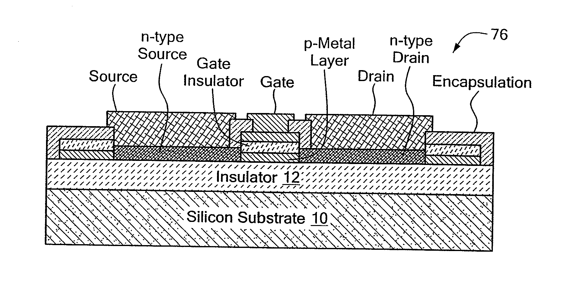
l view of a complementary version of the present invention. Either p-channel MOSFETs or p-channel metal transistors, as shown, can be integrated with n-channel metal transistors for complementary circuit designs.

[0015]FIG. 5 is a graphical illustration of examples of depletion width as a function of carrier concentration in the channel shown for difference values of relative dielectric constant K and effective voltage V.

[0016]FIG. 6 is a cross-sectional view of an enhancement-mode embodiment of this invention.

[0017]FIGS. 7A-7E is a series of cross-sectional views illustrating a process sequence for an enhancement-mode embodiment of this invention.

[0018]FIG. 8 is a process sequence for fabricating an integrated circuit device in accordance with the invention.

DETAILED DESCRIPTION OF THE INVENTION

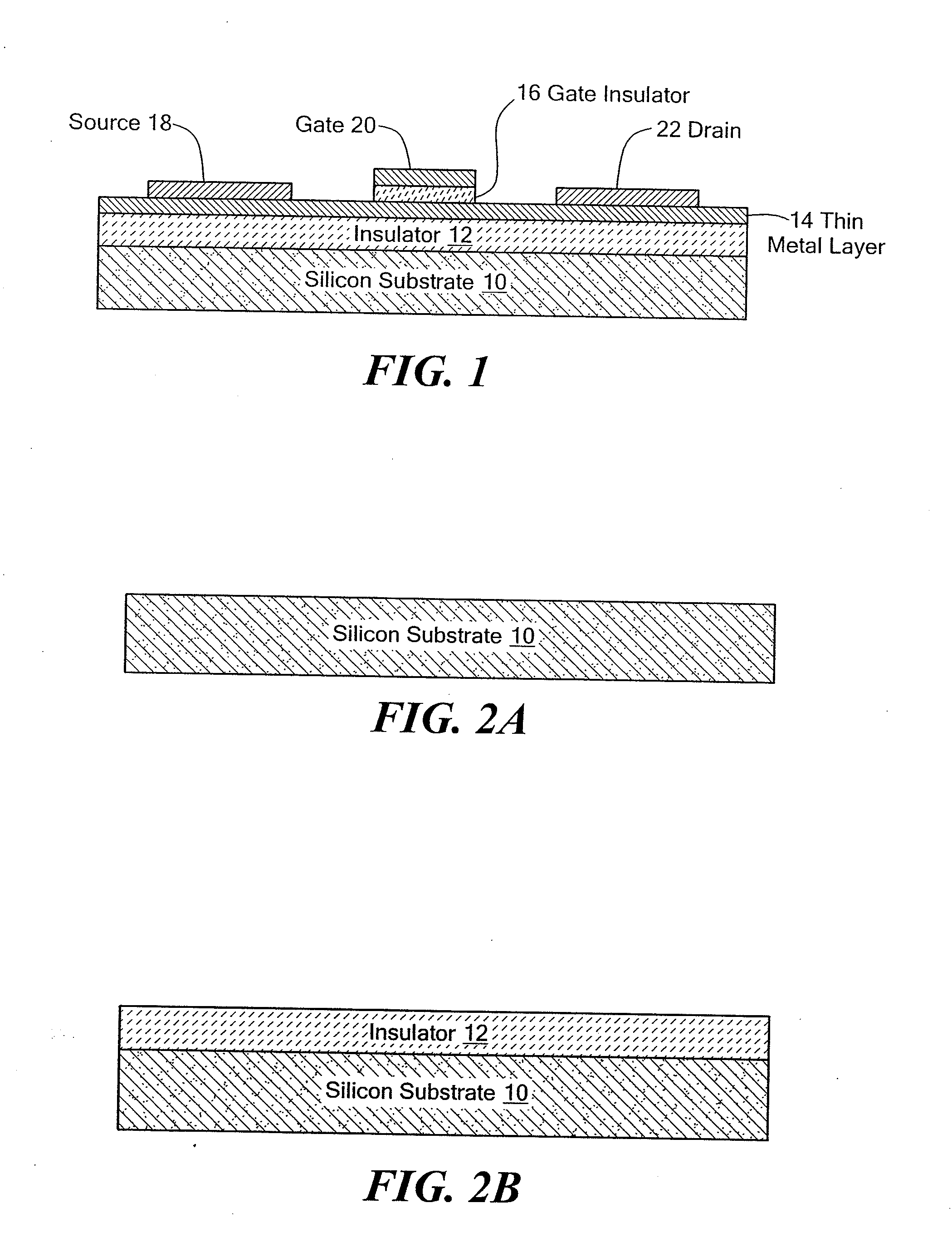
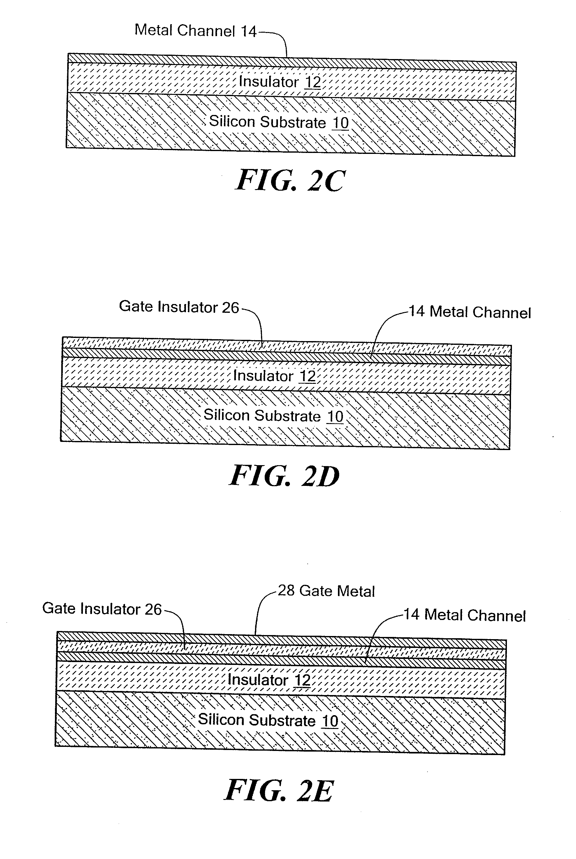
[0019]An invention is described herein to improve transconductance and reduce short channel effects over that of silicon transistors. A preferred embodiment of the invention uses a high conduc...


PUM

PropertyMeasurementUnit
thicknessaaaaaaaaaa
widthaaaaaaaaaa
widthaaaaaaaaaa

Abstract

The present invention is related to a depletion or enhancement mode metal transistor in which the channel regions of a transistor device comprises a thin film metal or metal composite layer formed over an insulating substrate.

Description

CROSS REFERENCE TO RELATED APPLICATIONS[0001]The present application is a continuation-in-part of, and claims priority to, U.S. patent application Ser. No. 10 / 762,658, filed Jan. 22, 2004 and claims benefit of U.S. Provisional Patent Application No. 60 / 441,931 filed Jan. 22, 2003 and U.S. Provisional Patent Application No. 60 / 477,983 filed Jun. 12, 2003. The entire contents of the above applications are incorporated herein by reference.BACKGROUND OF THE INVENTION[0002]As commercial integrated circuits push into 90-nm process technology with 50-nm gates and research devices push even smaller, further improvements in performance by scaling the channel length of transistors appear to be approaching the limits of scaling due to short channel, gate current leakage, and other effects. In particular, the power dissipation of integrated circuits is increasingly a problem as the transistor channel length is scaled down and transistors can no longer be completely shut off. Indeed the resultin...

Claims


Application Information

Patent Timeline
Patent Type & Authority Applications(United States)
IPC IPC(8): H01L29/78H01L21/8238H01L21/336H01L49/00
CPCH01L49/00H10N99/00
Inventor TSANG, DEAN Z.
Owner TSANG DEAN Z
Why Eureka
Try Eureka