Surface emitting semiconductor laser

a semiconductor laser and surface technology, applied in the direction of lasers, laser output parameters control, semiconductor lasers, etc., can solve the problems of reducing optical output and shortened li

Active Publication Date: 2011-07-28
FUJIFILM BUSINESS INNOVATION CORP
View PDF4 Cites 6 Cited by
  • Summary
  • Abstract
  • Description
  • Claims
  • Application Information

AI Technical Summary

Benefits of technology

[0008]According to an aspect of the present invention, there is provided a surface emitting semiconductor laser including: a substrate; a first semiconductor multilayer reflector of a first conduction type that is formed on the substrate and is composed of stacked pairs of relatively high refractive index layers and relatively low refractive index layers; a cavity region that is formed on the first semiconductor multilayer reflector and includes an active region; and a second semiconductor multilayer reflector of a second conduction type that is formed on the cavity region and is composed of stacked pairs of relatively high refractive index layers and relatively low refractive index layers, a cavity length of a cavity that includes the cavity region and the active region between the first semiconductor multilayer reflector and the second semiconductor multilayer reflector being greater than an oscillation wavelength, and the cavity region including an electrically conductive region of the first conduction type in proximity to the active region, and a low refractive index region that is interposed between the electrically conductive region and the first semiconductor multilayer reflector and has a smaller refractive index than that of the electrically conductive region.

Problems solved by technology

As the oxide aperture diameter reduces, the resistance of the laser increases and the heat generation temperature rises, so that life may be shortened.
Further, a reduced oxide aperture diameter results in a reduced optical output.

Method used


Image

  • Surface emitting semiconductor laser
  • Surface emitting semiconductor laser
  • Surface emitting semiconductor laser

Examples


Embodiment Construction

[0021]A description will now be given of exemplary embodiments of the present invention with reference to the accompanying drawings. In the following, surface emitting semiconductor lasers of selective oxidation type will be discussed and such lasers will now be referred to as VCSELs. The dimensions of VCSELs illustrated may be emphasized for the purpose of facilitating better understanding and may be different from the actual dimensions thereof.

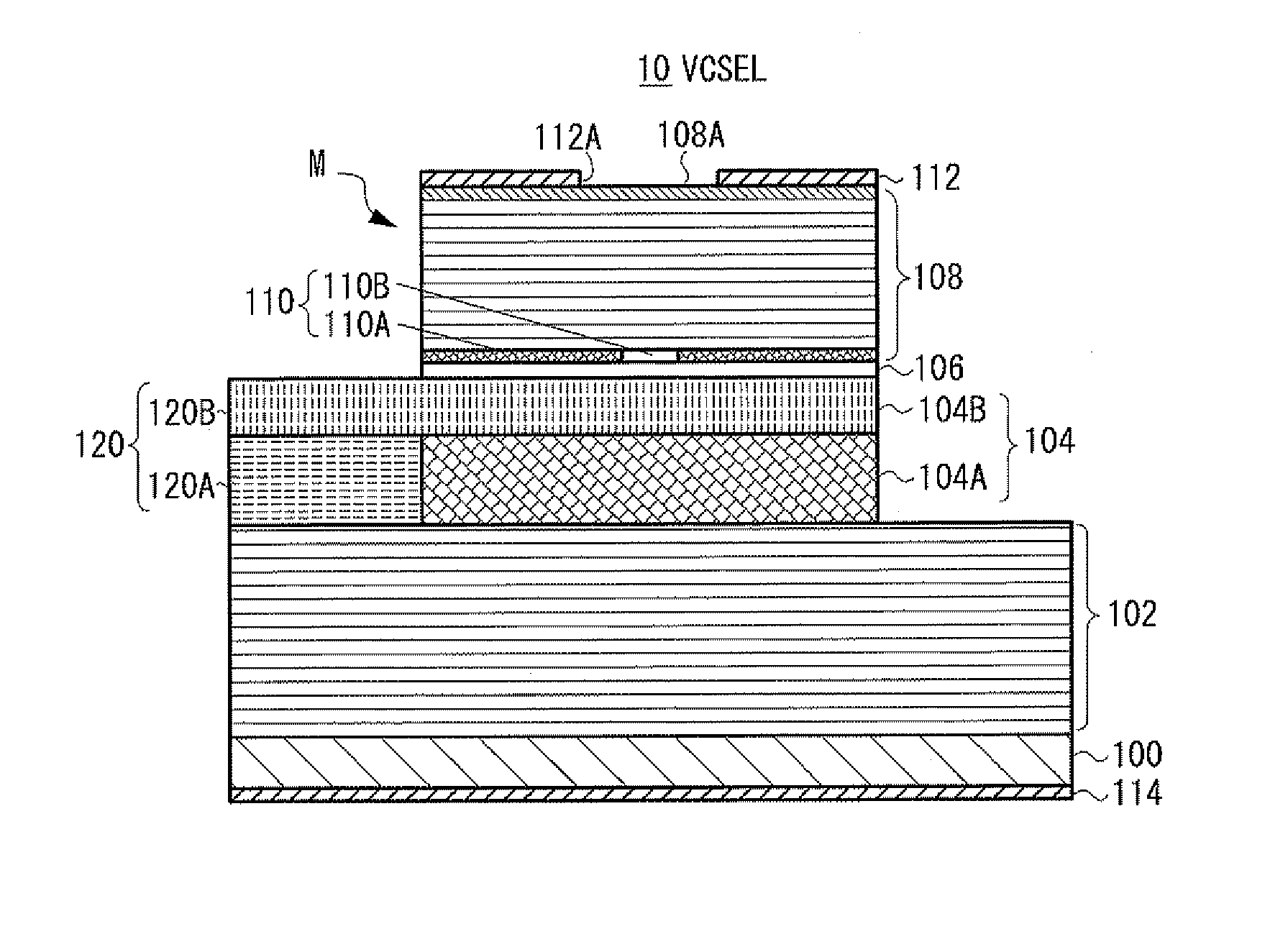
[0022]FIG. 1 is a cross-sectional view of a VCSEL in accordance with a first exemplary embodiment of the present invention. Referring to FIG. 1, a VCSEL 10 of the present exemplary embodiment has an n-type GaAs substrate 100 on which the following layers are stacked. An n-type lower distributed Bragg reflector (DBR) 102 formed by alternately staking AlGaAs layers having different Al compositions is provided on the n-type GaAs substrate 100. A cavity region 104, which extends a cavity length, is provided on the lower DBR 102. An active region...


PUM


Abstract

A surface emitting semiconductor laser includes: a substrate; a first semiconductor multilayer reflector of a first conduction type that is formed on the substrate and is composed of stacked pairs of relatively high refractive index layers and relatively low refractive index layers; a cavity region that is formed on the first semiconductor multilayer reflector and includes an active region; and a second semiconductor multilayer reflector of a second conduction type that is formed on the cavity region and is composed of stacked pairs of relatively high refractive index layers and relatively low refractive index layers. A cavity length of a cavity that includes the cavity region and the active region between the first semiconductor multilayer reflector and the second semiconductor multilayer reflector is greater than an oscillation wavelength.

Description

CROSS-REFERENCE TO RELATED APPLICATION[0001]This application is based on and claims priority under 35 USC 119 from Japanese Patent Application No. 2010-015722 filed on Jan. 27, 2010.BACKGROUND[0002](i) Technical Field[0003]The present invention relates to a surface emitting semiconductor laser, a surface emitting semiconductor laser device, an optical transmission device and an information processing apparatus.[0004](ii) Related Art[0005]A surface emitting semiconductor laser, which is typically a vertical cavity surface emitting laser: VCSEL), is utilized as an optical source in a communication device and an image forming apparatus. The VCSEL used as the optical source is required to have improved optical output and electro static discharge (ESD) in the single transverse mode and to have lengthened life by reducing the resistance and heat radiation performance.[0006]A typical selective oxidation type VCSEL has a current confining layer in which an oxide aperture formed by selective...

Claims


Application Information

Patent Timeline
Patent Type & Authority Applications(United States)
IPC IPC(8): H01S5/06
CPCH01S5/02284H01S5/02288H01S5/0655B82Y20/00H01S5/18313H01S5/18358H01S5/3432H01S5/1039H01S5/02251H01S5/02253
Inventor KONDO, TAKASHITAKEDA, KAZUTAKA
Owner FUJIFILM BUSINESS INNOVATION CORP
Why Eureka
Try Eureka