Light-emitting device and production method therefor

a technology of light-emitting devices and production methods, which is applied in the direction of semiconductor devices, basic electric elements, electrical apparatus, etc., can solve the problems of reduced light extraction efficiency of conventional light-emitting devices, and the light generated in the light-emitting layer is not completely extracted, so as to facilitate light extraction to the outside and suppress light absorption by electrodes

Inactive Publication Date: 2017-03-23
TOYODA GOSEI CO LTD
View PDF3 Cites 5 Cited by
  • Summary
  • Abstract
  • Description
  • Claims
  • Application Information

AI Technical Summary

Benefits of technology

[0007]The present technique has been conceived in order to solve the aforementioned problems involved in conventional techniques. Thus, an object of the present technique is to provide a light-emitting device which realizes suppression of light absorption by electrodes as well as easy light extraction. Another object is to provide a production method therefor.
[0009]In the light-emitting device, the refractive index decreases in the direction from the Group III nitride semiconductor layer, the transparent conductive oxide film, the first dielectric film, and the phosphor-containing resin coating. The light emitted by the light-emitting layer passes sequentially through the Group III nitride semiconductor layer, the transparent conductive oxide film, the first dielectric film, and the phosphor-containing resin coating. Thus, the light emitted by the light-emitting device can be extracted to the outside, with total reflection being prevented to a certain extent. Also, the refractive index of the current-blocking layer is smaller than that of the phosphor-containing resin coating. Thus, the light which is emitted by the Group III nitride semiconductor layer and enters the transparent conductive oxide film via the current-blocking layer tends to be reflected by the interface between the current-blocking layer and the transparent conductive oxide film. Accordingly, the light passing through the route to the outside is not likely to be reflected inside the light-emitting device, while the light moving toward electrodes is readily reflected inside the light-emitting device. Therefore, the emitted light is not completely absorbed by the electrodes and can be extracted to the outside. As a result, the light-emitting device of the present technique exhibits excellent light extraction efficiency.
[0017]According to the light-emitting device of the present technique and the production method therefor, light absorption by electrodes can be suppressed, and light extraction to the outside can be facilitated.

Problems solved by technology

However, the light generated in the light-emitting layer is not completely extracted from the Group III nitride semiconductor light-emitting device to the outside.
Thus, the conventionally developed light-emitting devices exhibit reduced light extraction efficiency.

Method used


Image

  • Light-emitting device and production method therefor
  • Light-emitting device and production method therefor
  • Light-emitting device and production method therefor

Examples


first embodiment

1. Light-Emitting Device

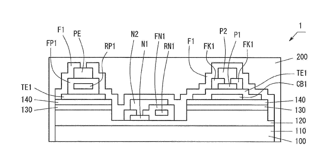
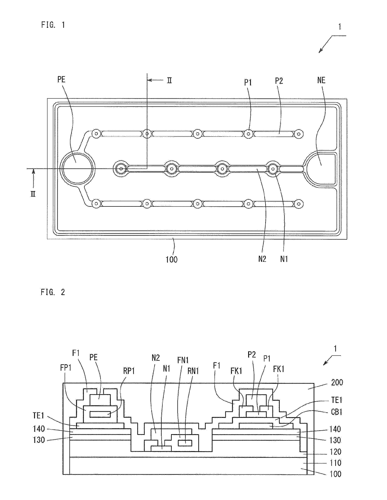
[0033]FIG. 1 is plan view showing the structure of a light-emitting device 1 according to the first embodiment. FIG. 2 is a cross-section of the light-emitting device 1 shown in FIG. 1, cut along II-II. The light-emitting device 1 has a light-emitting element 100 and a phosphor-containing resin coating 200. The light-emitting device 1 is a Group III nitride semiconductor light-emitting device which emits white light. The light-emitting device 1 provides light having a wavelength of 400 nm to 800 nm. The light-emitting element 100 is a semiconductor light-emitting device of face-up type having a plurality of semiconductor layers formed of a Group III nitride semiconductor.

[0034]As shown in FIGS. 1 and 2, the light-emitting element 100 has a substrate 110, an n-type semiconductor layer 120, a light-emitting layer 130, a p-type semiconductor layer 140, a current-blocking layer CB1, a transparent conductive oxide film TE1, a dielectric film F1, a dielectric film ...

second embodiment

[0082]Second embodiment will be described.

1. Light-Emitting Device

[0083]FIG. 11 is a plan view of the general structure of a light-emitting device 3 of the second embodiment, and FIG. 12 is a cross-section of the light-emitting device 3 shown in FIG. 11, cut along XII-XII. The light-emitting device 3 has a light-emitting element 400 and a phosphor-containing resin coating 200.

[0084]As shown in FIGS. 11 and 12, the light-emitting element 400 has a substrate 110, an n-type semiconductor layer 120, a light-emitting layer 130, a p-type semiconductor layer 140, a current-blocking layer CB1, a transparent conductive oxide film TE1, a dielectric film F2, a dielectric film FN1, a dielectric film FP1, a dielectric film FK1, a reflective film RN1, a reflective film RP1, n-side dot electrodes N1, an n-side wiring electrode N2, an n-side pad electrode NE, p-side dot electrodes P1, a p-side wiring electrode P2, and a p-side pad electrode PE.

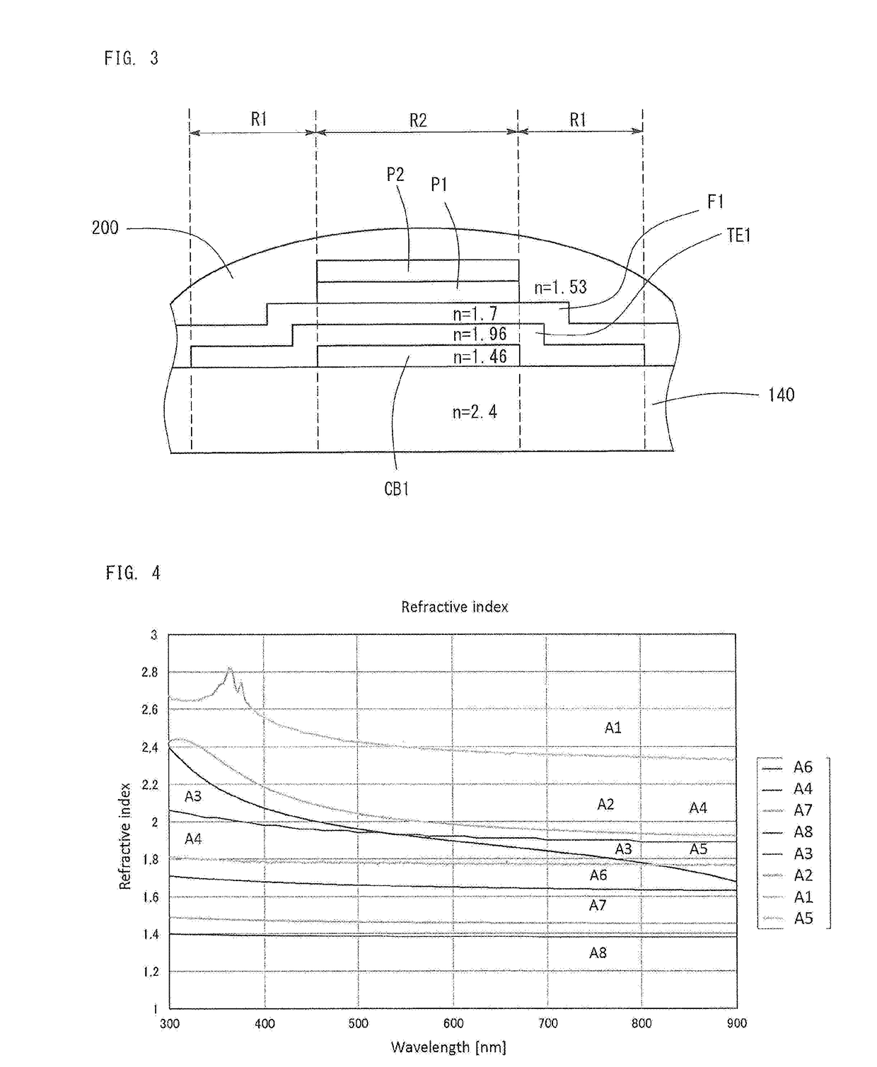
2. Relationship Between Stacking Configuration and Refr...

third embodiment

[0088]Third embodiment will be described.

1. Light-Emitting Device

[0089]FIG. 13 is a cross-section of the light-emitting device 4 of the third embodiment. The light-emitting device 4 has a light-emitting element 500 and a phosphor-containing resin coating 200.

[0090]As shown in FIG. 13, the light-emitting element 500 has a substrate 110, an n-type semiconductor layer 120, a light-emitting layer 130, a p-type semiconductor layer 140, a distributed Bragg reflector DBR1, a transparent conductive oxide film TE1, a distributed Bragg reflector DBR2, a distributed Bragg reflector DBR3, a dielectric film F3, n-side dot electrodes N1, an n-side wiring electrode N2, an n-side pad electrode NE, p-side dot electrodes P1, a p-side wiring electrode P2, and a p-side pad electrode PE.

[0091]The distributed Bragg reflectors DBR1, DBR2, and DBR3 serve as films each selectively reflecting light having a wavelength λ. The dielectric film F3 serves as an anti-reflector (AR).

[0092]Thus, when the distributed...


PUM

PropertyMeasurementUnit
emission wavelengthaaaaaaaaaa
light wavelengthaaaaaaaaaa

Abstract

The light-emitting device of the present technique includes a substrate, a Group III nitride semiconductor layer disposed on the substrate, a current-blocking layer disposed on the Group III nitride semiconductor layer, a transparent conductive oxide film disposed on the Group III nitride semiconductor layer and the current-blocking layer, a dielectric film covering the Group III nitride semiconductor layer and at least a part of the transparent conductive oxide film, and a phosphor-containing resin coating disposed on the dielectric film. The Group III nitride semiconductor layer has a refractive index greater than that of the transparent conductive oxide film. The transparent conductive oxide film has a refractive index greater than that of the dielectric film. The dielectric film has a refractive index greater than that of the phosphor-containing resin coating. The current-blocking layer has a refractive index smaller than that of the phosphor-containing resin coating.

Description

BACKGROUND OF THE INVENTION[0001]Field of the Invention[0002]The present technique relates to a light-emitting device and to a method for producing the device.[0003]Background Art[0004]Generally, a Group III nitride semiconductor light-emitting device has a light-emitting layer which emits light through recombination of electrons and holes, an n-type semiconductor layer, and a p-type semiconductor layer. However, the light generated in the light-emitting layer is not completely extracted from the Group III nitride semiconductor light-emitting device to the outside. The light is partially absorbed by members of the Group III nitride semiconductor light-emitting device, or reflected by members of the Group III nitride semiconductor light-emitting device.[0005]In order to solve the problem, some techniques have been developed for suitably extracting light from Group III nitride semiconductor light-emitting devices. Among them, Patent Document 1 discloses a technique of forming a transp...

Claims


Application Information

Patent Timeline
Patent Type & Authority Applications(United States)
IPC IPC(8): H01L33/14H01L33/04H01L33/46H01L33/00H01L33/32H01L33/42
CPCH01L33/145H01L33/32H01L33/04H01L33/46H01L33/0075H01L33/42H01L33/005H01L33/14H01L33/44H01L33/38H01L33/50
Inventor GOSHONOO, KOICHITOTANI, SHINGO
Owner TOYODA GOSEI CO LTD
Why Eureka
Try Eureka