High efficiency solar cell device with gallium arsenide absorber layer

a solar cell and absorber layer technology, applied in the field of solar cells, can solve the problems of low device stability, deformation of absorber layer, deformation of film solar cells, etc., and achieve the effect of improving light absorption and conversion efficiency

Inactive Publication Date:
View PDF4 Cites 13 Cited by
  • Summary
  • Abstract
  • Description
  • Claims
  • Application Information

AI Technical Summary

Benefits of technology

[0008]Embodiments of the invention provide a method of forming a gallium arsenide based (GaAs) layer with or without dopants from a solution based precursor. The gallium arsenide based (GaAs) layer formed from the solution based precursor may be incorporated in solar cell devices to improve light absorption and conversion efficiency. In one embodiment, a method of forming a solar cell device includes forming a first layer with a first type of dopants doped therein over a surface of a substrate, forming a GaAs based layer on the first layer, and forming a second layer with a second type of dopants doped therein on the GaAs based layer.

Problems solved by technology

It has been found that the properties of thin-film solar cells degrade over time upon exposure to light, which can cause the device stability to be less than desired.
However, some absorber layers are often defective with high densities of recombination sites that have a significant detrimental effect on the efficiency of the solar devices.

Method used


Image

  • High efficiency solar cell device with gallium arsenide absorber layer
  • High efficiency solar cell device with gallium arsenide absorber layer
  • High efficiency solar cell device with gallium arsenide absorber layer

Examples


Embodiment Construction

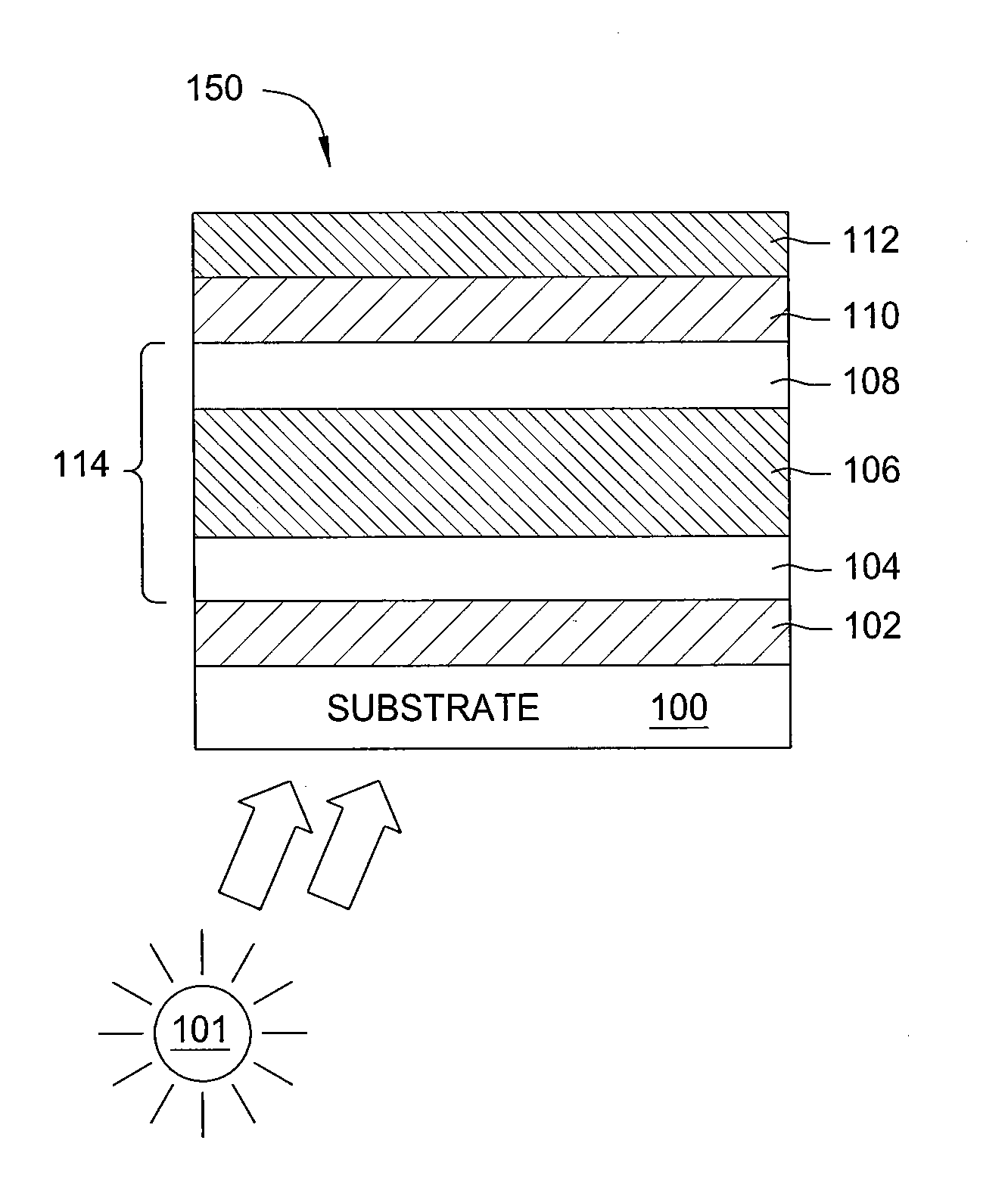
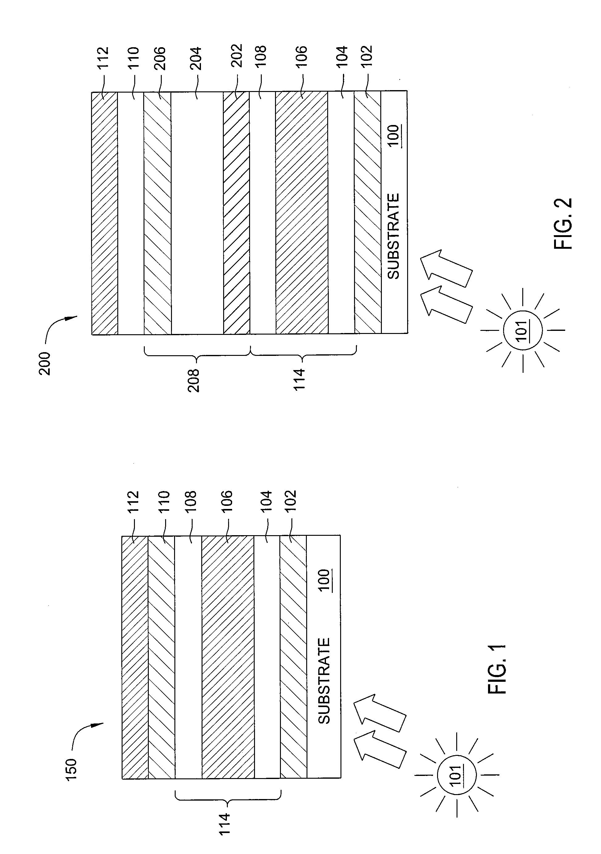
[0023]Solar cell devices that are formed using thin film deposition processes generally comprise numerous layers of material, or films, of differing composition that can be put together in many different ways. Most films used in such devices incorporate a semiconductor element that may comprise silicon, germanium, gallium, arsenide, indium, carbon, boron, phosphorous, nitrogen, oxygen, hydrogen and the like. Characteristics of the different deposited films include degrees of crystallinity, dopant type, dopant concentration, band gap, film refractive index, film extinction coefficient, film transparency, film absorption, and conductivity.

[0024]Charge generation during a photovoltaic process is generally provided by one or more light absorber layers. Typically, the electron-hole pair generation process predominantly occurs in an intrinsic layer that is used to space the oppositely doped p-n regions of a p-i-n type thin film solar cell device apart. The phrase “intrinsic layer” is typi...


PUM

PropertyMeasurementUnit
temperatureaaaaaaaaaa

Abstract

Embodiments of the invention provide a method of forming a doped gallium arsenide based (GaAs) layer from a solution based precursor. The doped gallium arsenide based (GaAs) layer formed from the solution based precursor may assist solar cell devices to improve light absorption and conversion efficiency. In one embodiment, a method of forming a solar cell device includes forming a first layer with a first type of dopants doped therein over a surface of a substrate, forming a GaAs based layer on the first layer, and forming a second layer with a second type of dopants doped therein on the GaAs based layer.

Description

CROSS-REFERENCE TO RELATED APPLICATIONS[0001]This application claims benefit of U.S. Provisional Application Ser. No. 61 / 388,943 filed Oct. 1, 2010 (Attorney Docket No. APPM / 15444L), U.S. Provisional Application Ser. No. 61 / 452,801 filed Mar. 15, 2011 (Attorney Docket No. APPM / 15444L02) and U.S. Provisional Application Ser. No. 61 / 468,918, filed Mar. 29, 2011 (Attorney Docket No. APPM / 15444L03), all of which are incorporated by reference in their entirety.BACKGROUND OF THE INVENTION[0002]1. Field of the Invention[0003]Embodiments of the present invention generally relate to solar cells and methods for forming the same. More particularly, embodiments of the present invention relate to a gallium arsenide (GaAs) based solar cells.[0004]2. Description of the Related Art[0005]Solar cells convert solar radiation and other light into usable electrical energy. The energy conversion occurs as the result of the photovoltaic effect. Solar cells may be formed from crystalline material or from a...

Claims


Application Information

Patent Timeline
Patent Type & Authority Applications(United States)
IPC IPC(8): H01L31/0264H01L31/18B82Y40/00
CPCB82Y30/00B82Y10/00C23C16/56H01L21/0237H01L21/02491H01L21/02546H01L21/02576H01L21/02579H01L21/02601H01L21/0262H01L21/02628H01L31/022425H01L31/035227H01L31/072H01L31/075H01L31/184H01L31/1864H01L51/0048H01L51/424Y02E10/544Y02E10/548Y02E10/549C23C16/301Y02P70/50H10K85/221H10K30/20H01L31/0264H01L31/18H01L31/04H01L21/02631H01L21/3245H01L27/1225H01L27/127H01L29/207H01L29/454H01L29/66742H01L29/78618H01L29/78681H01L29/78696
Inventor SINGH, KAUSHAL K.VISSER, ROBERT JANRAO, SRIKANTKUMAR, BHASKARCARMALT, CLAIRE J.ARNEPALLI, RANGA RAONALAMASU, OMKARAMSARAF, GAURAVSATHASIVAM, SANJAYANBLACKMAN, CHRISTOPHER STUART
Why Eureka
Try Eureka