

Photodetector
a photodetector and photosensor technology, applied in the field of photodetectors, can solve the problems of cumbersome use of the photodetector and intrinsically low photosensitivity, and achieve the effect of high photosensitivity
- Summary
- Abstract
- Description
- Claims
- Application Information
AI Technical Summary
Benefits of technology
Problems solved by technology
Method used
Image

Examples
first embodiment
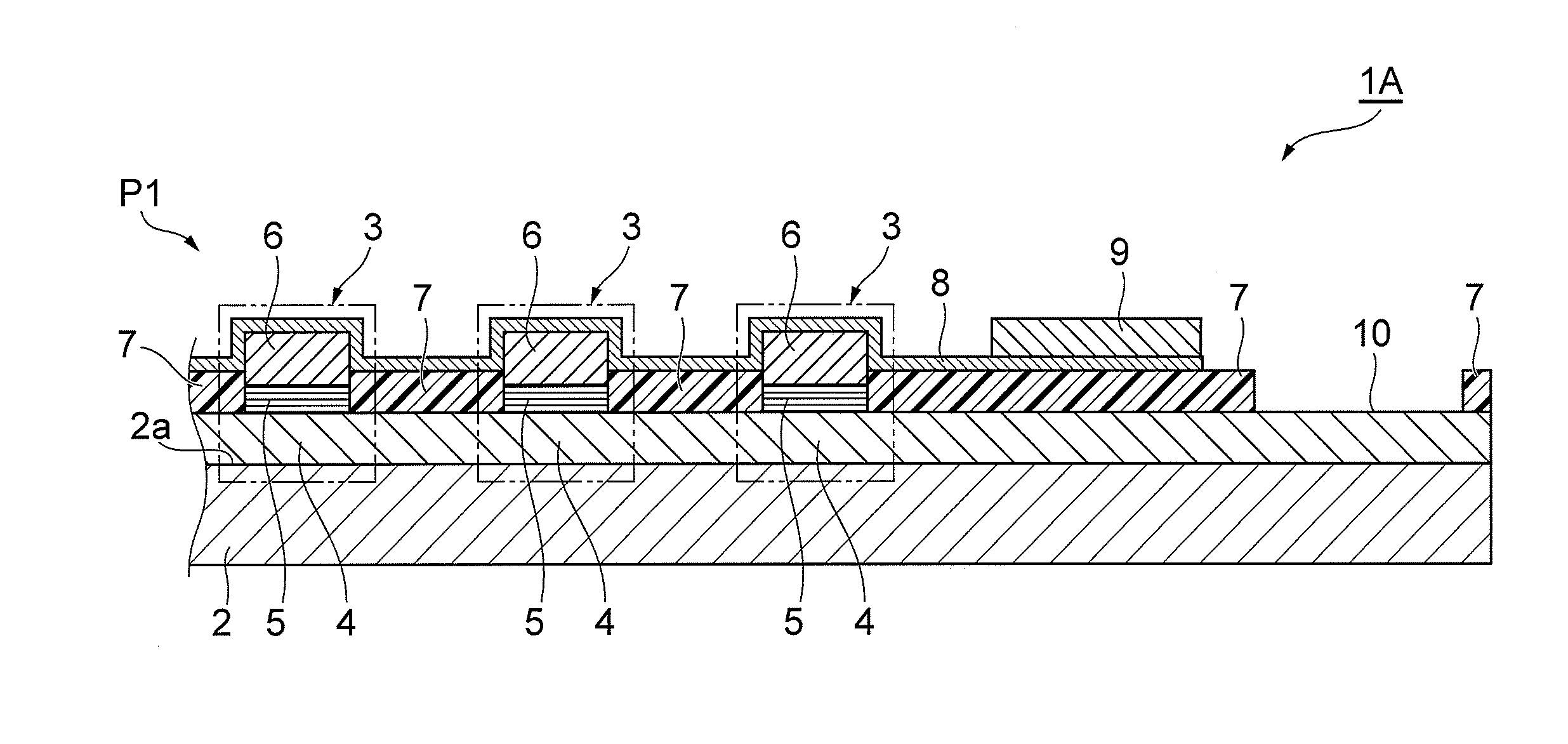
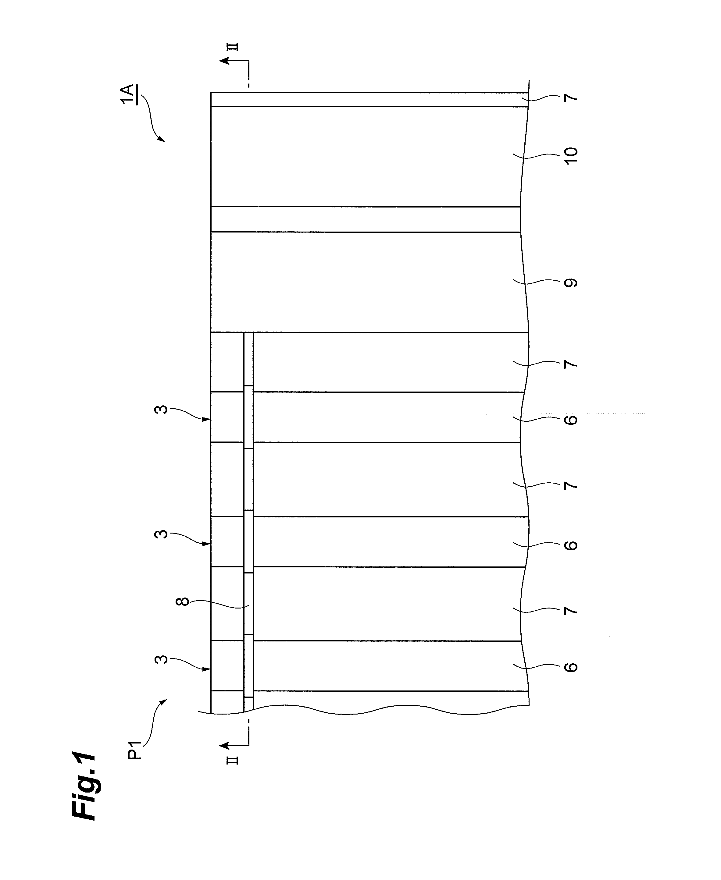
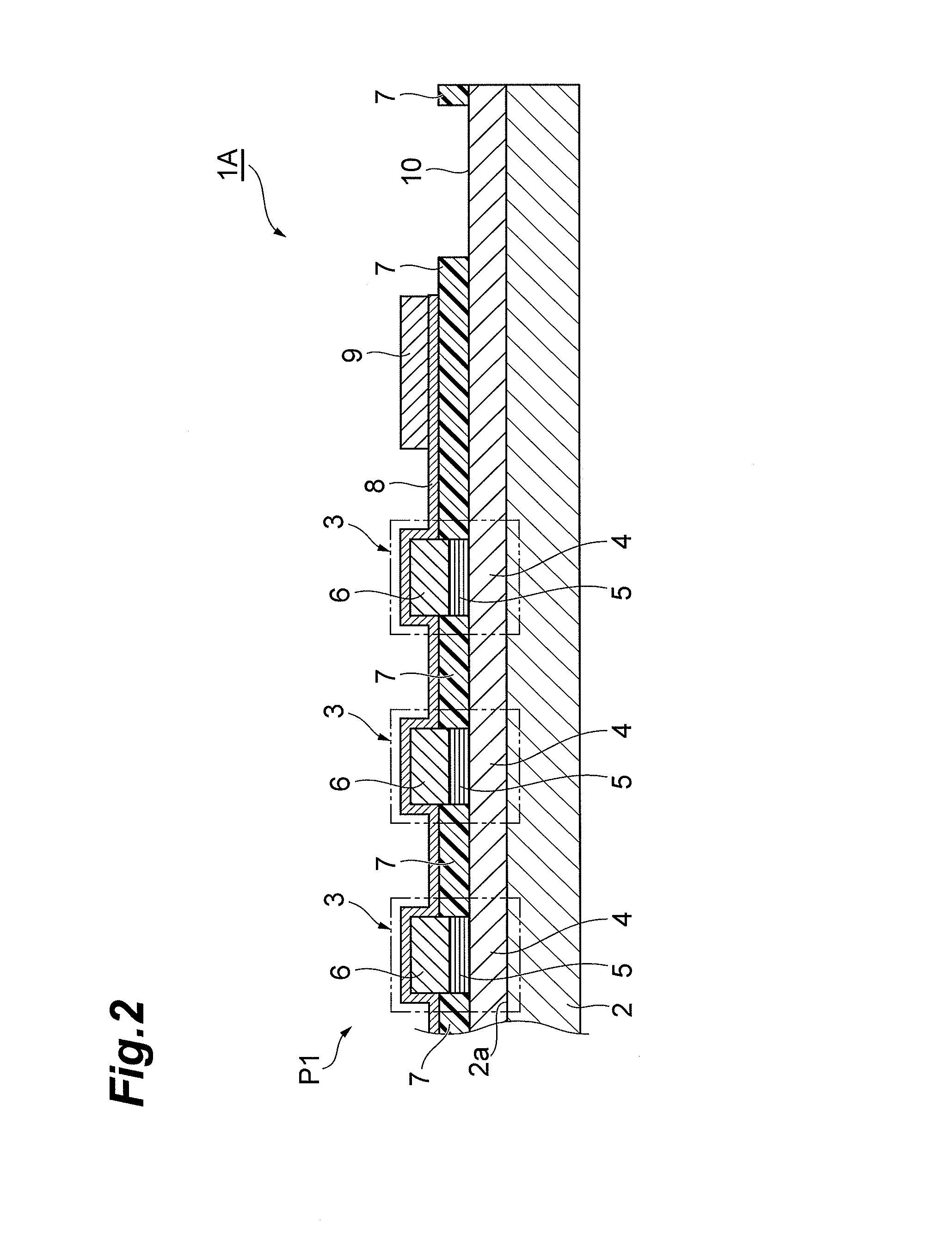
[0052]As illustrated in FIGS. 1 and 2, a photodetector 1A comprises a substrate 2 made of a semiconductor such as InP, GaAs, or Si or SiO2 (glass) and a plurality of multilayer structures 3 arranged on a principal surface 2a thereof.
[0053]Each multilayer structure 3 comprises a first metal layer (first layer) 4 constituted by first metal such as Au, Ag, or Al; a semiconductor structure layer 5 mounted on the first metal layer 4 and adapted to excite electrons in response to light incident thereon and its resulting plasmon resonance; and a second metal layer (second layer) 6 mounted on the semiconductor structure layer 5 and constituted by second metal such as Au, Ag, or Al. The plurality of multilayer structures 3 are arranged such that a periodic pattern P1 is formed like stripes along a plane perpendicular to the stacking direction of the first metal layer 4, semiconductor structure layer 5, and second metal layer 6 on the substrate 2 in a planar view. That is, the periodic patter...
second embodiment
[0071]Another mode of the photodetector will be explained as the second embodiment of the present invention. As illustrated in FIGS. 13 and 14, the photodetector 1B of the second embodiment differs from the photodetector 1A of the first embodiment in the form and arrangement of multilayer structures in a planar view.
[0072]In the photodetector 1B, a plurality of multilayer structures 23, each having a second metal layer 26 and a semiconductor structure layer 25 which are square in a planar view, are arranged like islands in a square lattice, so as to construct a periodic pattern P2. That is, the periodic pattern P2 is patterned two-dimensionally along a plane perpendicular to the stacking direction of the multilayer structures 23.
[0073]While the photodetector 1A of the first embodiment has the multilayer structure 3 capable of acting as a cavity for causing surface plasmon resonance in only one direction (the direction in which stripe-shaped periodic pattern P1 arranged in a row) and...
third embodiment
[0074]Another mode of the photodetector will be explained as the third embodiment of the present invention. As illustrated in FIGS. 15 and 16, the photodetector 1C of the third embodiment differs from the photodetector 1B of the second embodiment in that it includes a plurality of sizes of multilayer structures.
[0075]A periodic pattern P3 in the photodetector 1C includes a plurality of periodic pattern parts P3a, P3b, P3c having different sizes of second metal layers 36a, 36b, 36c and semiconductor structure layers 35a, 35b, 35c. That is, as illustrated in FIG. 15, multilayer structures 33a, 33b, 33c form the first periodic pattern part P3a, second periodic pattern part P3b, third periodic pattern part P3c which are distinguished from one another by different sizes of the second metal layers 36a, 36b, 36c and semiconductor structure layers 35a, 35b, 35c, while their respective periodic pattern parts P3a, P3b, P3c are each patterned one-dimensionally along a plane perpendicular to th...
PUM
| Property | Measurement | Unit |
|---|---|---|
| total thickness | aaaaa | aaaaa |
| total thickness | aaaaa | aaaaa |
| wavelength | aaaaa | aaaaa |
Abstract
Description
Claims
Application Information