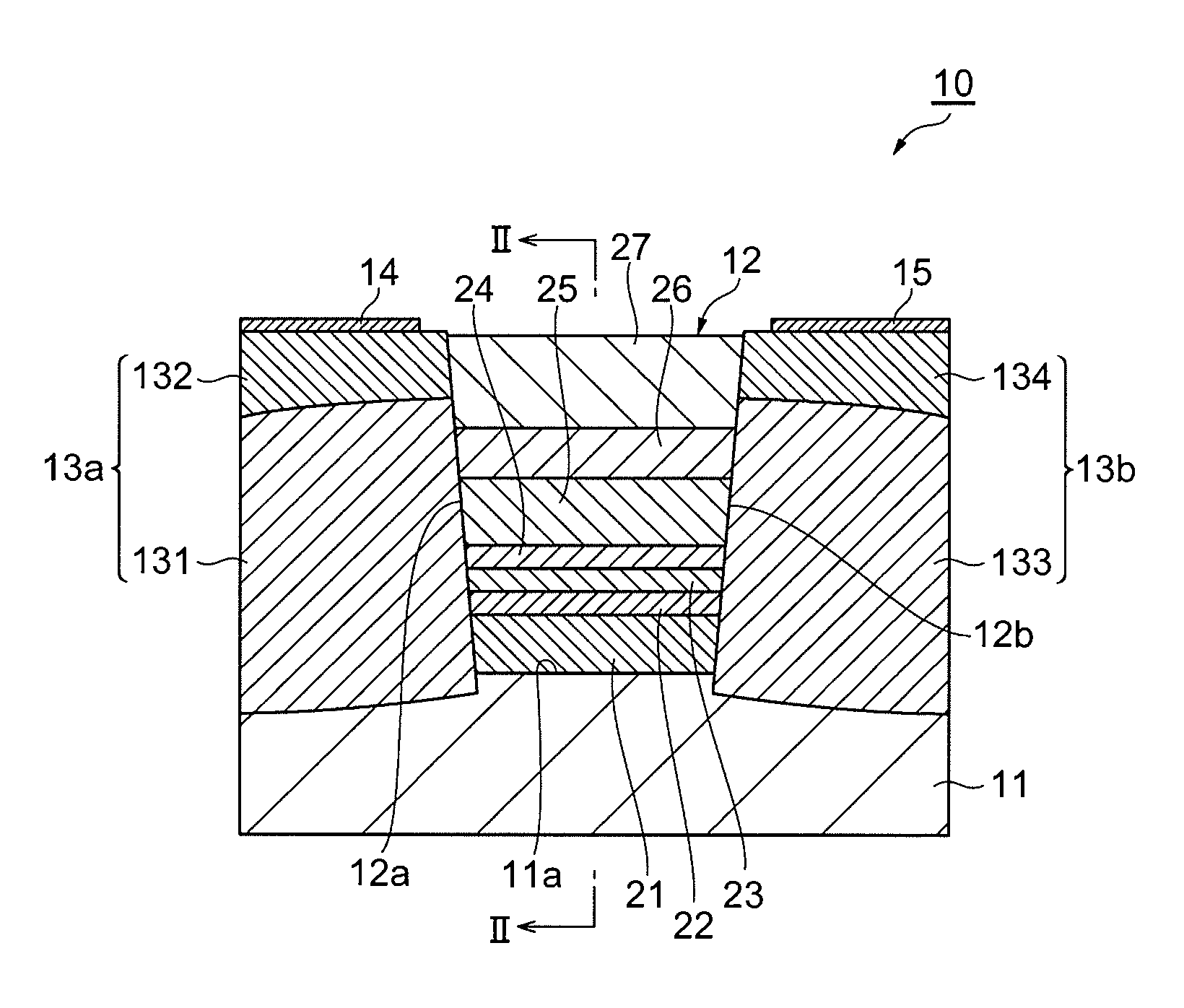
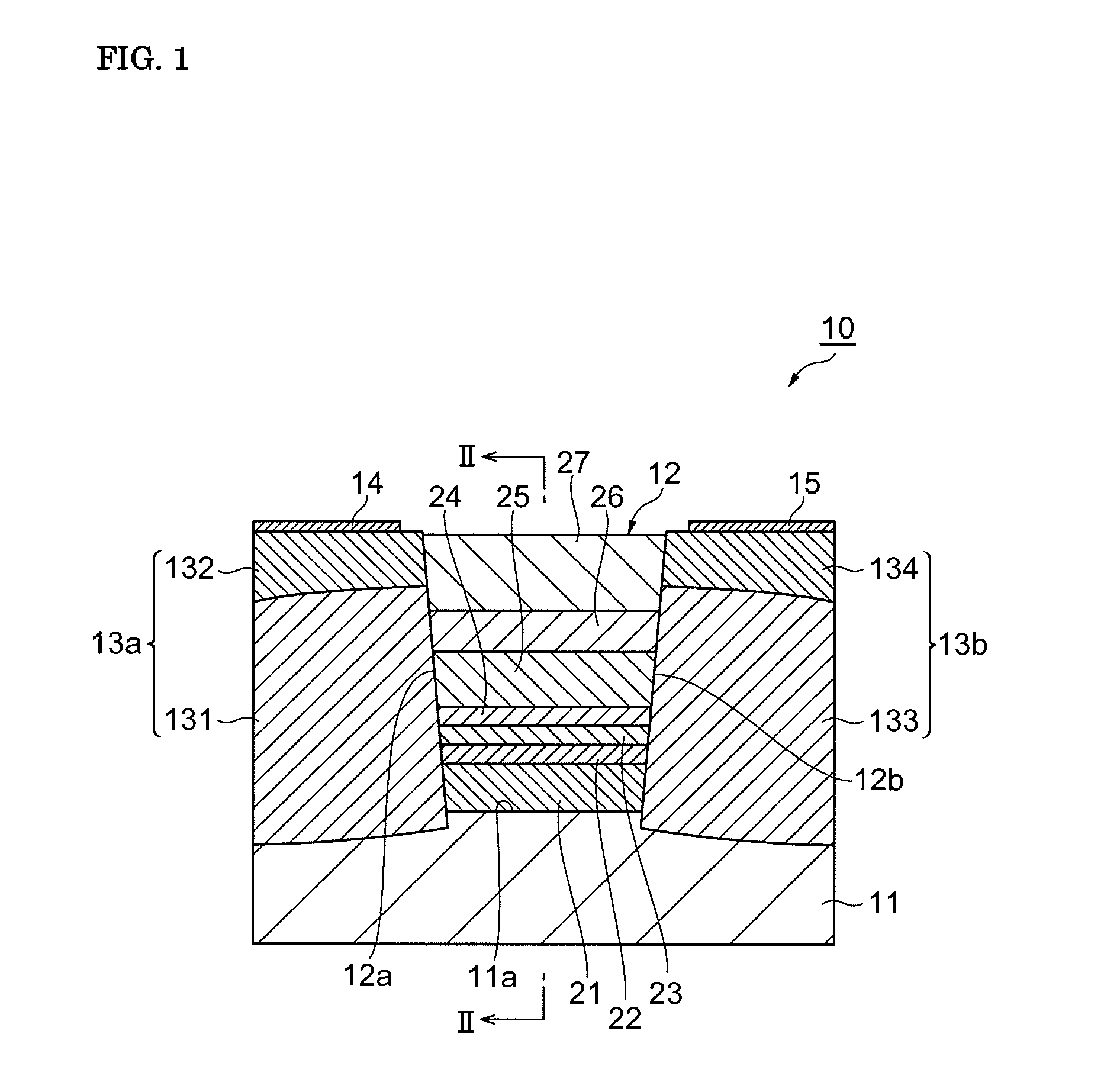
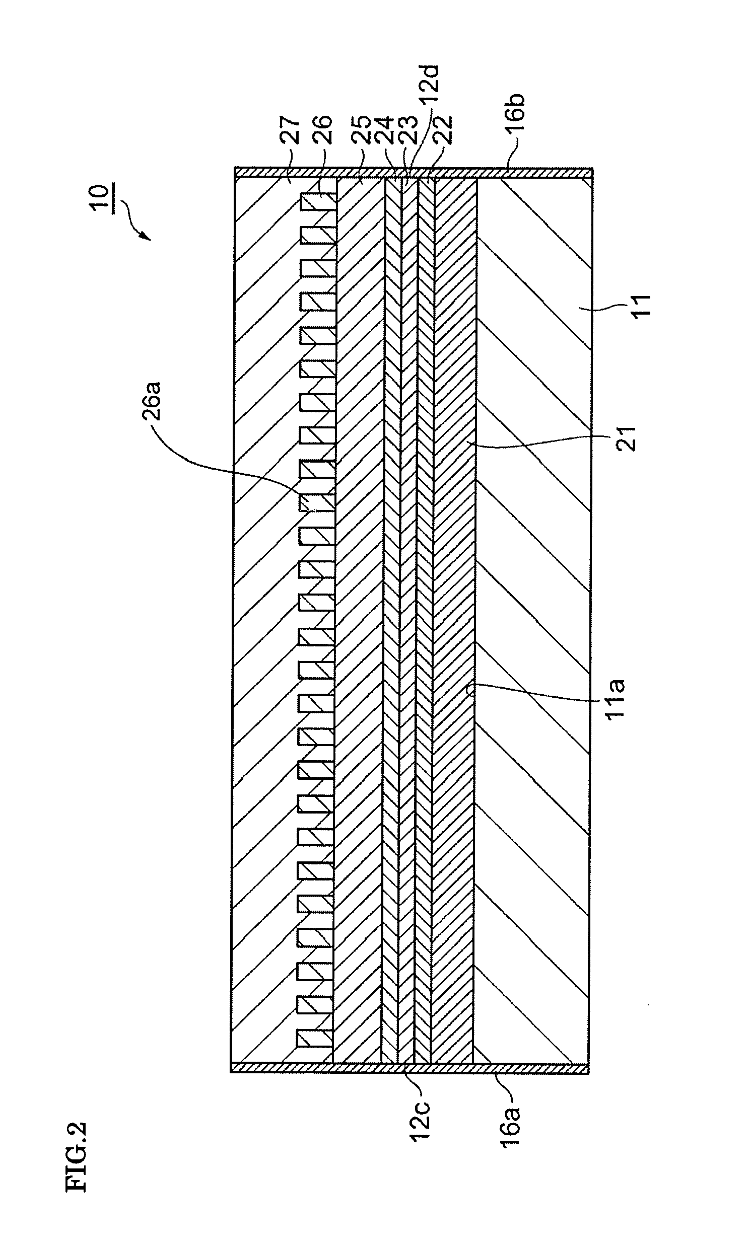
[0007]The semiconductor laser device according to the embodiment includes the first optical waveguide constituted by the lower cladding layer, the active layer, and the upper cladding layer; and the second optical waveguide constituted by the upper cladding layer, the diffraction-grating layer, and the buried layer. The active layer constitutes a first core region in the first optical waveguide. The diffraction-grating layer constitutes a second core region in the second optical waveguide. The first optical waveguide and the second optical waveguide are optically coupled with each other through the upper cladding layer. The diffraction-grating layer includes periodic projections and recesses arranged in the
light propagation direction. The buried layer is disposed on the periodic projections and recesses in the diffraction-grating layer. In the semiconductor laser device according to the embodiment, light generated in the active layer propagates through the first optical waveguide. That is, this optical guided mode (hereafter, referred to as an active-layer mode) propagates through the first optical waveguide including the active layer as the first core region. In addition to this active-layer mode, another optical guided mode (hereafter, referred to as a diffraction-grating-layer mode) propagates through the second optical waveguide including the diffraction-grating layer as the second core region. The
dispersion curve of the active-layer mode is different from that of the diffraction-grating-layer mode. The active-layer mode and the diffraction-grating-layer mode being in proximity to each other propagate in the first optical waveguide and the second optical waveguide, respectively. A
phase matching condition for lasing is satisfied at a
wavelength at which the
dispersion curve of the active-layer mode and the
dispersion curve of the diffraction-grating-layer mode intersect. Lasing occurs at this specific
wavelength (single
wavelength) at which the
phase matching condition is satisfied. The wavelength of light propagating at the diffraction-grating-layer mode depends on the period of the
diffraction grating. The active layer (the first core region) of the first optical waveguide and the diffraction-grating layer (the second core region) of the second optical waveguide are spatially separated from each other through the upper cladding layer therebetween. When a current is injected into the active layer, the
refractive index of the active layer changes. Then, the dispersion curve of the active-layer mode propagating through the first optical waveguide changes. However, even when a current is injected into the active layer, the
refractive index of the diffraction-grating layer almost does not change because a current is not injected into the diffraction-grating layer. As a result, the dispersion curve of the diffraction-grating-layer mode propagating through the second optical waveguide almost does not change. Furthermore, the wavelength of light at the point where the dispersion curves of the first and second optical waveguides intersect almost does not change. Therefore, in the semiconductor laser device according to the embodiment, even when a modulated current is injected into the active layer, variation in the
lasing wavelength can be reduced and wavelength chirping can be suppressed.
[0009]In the semiconductor laser device according to the embodiment, the buried layer may be composed of a
dielectric material.
Dielectric materials have a
refractive index considerably lower than the refractive index of semiconductors. Accordingly, by forming the buried layer with a
dielectric material, the refractive index difference between the buried layer and the diffraction-grating layer can be increased. As a result, the diffraction-grating-layer mode propagating through the second optical waveguide is
strongly coupled to the diffraction grating. The
coupling coefficient κ between the diffraction-grating-layer mode and the diffraction grating is increased. By increasing the
coupling coefficient κ between the diffraction-grating-layer mode and the diffraction grating, variation in the wavelength of the dispersion curve of the diffraction-grating-layer mode can be reduced with respect to variation in the
propagation constant. As a result, the influence of variation in the refractive index of the active layer on the
lasing wavelength can be further reduced. Therefore, in the semiconductor laser device, wavelength chirping can be further suppressed. The
dielectric material may contain at least one of SiO2, SiN, Al2O3, and TiO.
[0011]In the semiconductor laser device according to the embodiment, a
relative refractive index difference (n1−n0) / n1 may be 0.15 or more where n1 represents a refractive index of the diffraction-grating layer and n0 represents a refractive index of the buried layer. When the
relative refractive index difference between the diffraction-grating layer and the buried layer is 0.15 or more, the
coupling coefficient κ between the diffraction-grating-layer mode and the diffraction grating is sufficiently increased and the influence of variation in the refractive index of the active layer on the
lasing wavelength can be effectively reduced. Therefore, in the semiconductor laser device, wavelength chirping can be further effectively suppressed.
[0012]In the semiconductor laser device according to the embodiment, the upper cladding layer may have a thickness of 500 nm or more and 1500 nm or less. The thickness of the upper cladding layer relates to the distance between the first core region (the active layer) of the first optical waveguide and the second core region (the diffraction-grating-layer) of the second optical waveguide. By forming the upper cladding layer so as to have a thickness of 500 nm or more, the active-layer mode propagating through the first optical waveguide and the diffraction-grating-layer mode propagating through the second optical waveguide can be readily formed. By optically coupling the first optical waveguide and the second optical waveguide, the active-layer mode and the diffraction-grating-layer mode interact with each other to achieve lasing. When the thickness of the upper cladding layer is more than 1500 nm, the
optical coupling between the first optical waveguide and the second optical waveguide becomes weak and hence it becomes difficult to achieve lasing with the active-layer mode and the diffraction-grating-layer mode interacting with each other.
[0013]In the semiconductor laser device according to the embodiment, the diffraction-grating layer may have a thickness of 200 nm or more. By forming the diffraction-grating layer so as to have such a large thickness, the diffraction-grating-layer mode can be suitably formed. For the diffraction-grating layer having such a large thickness, the periodic projections and recesses formed in the diffraction-grating layer can have a large height or large depth. The buried layer is disposed on the periodic projections and recesses. Furthermore, the buried layer has the refractive index remarkably smaller than that of the diffraction-grating layer. In this case, the coupling coefficient κ between the diffraction-grating-layer mode and the diffraction grating can be sufficiently increased. Therefore, the influence of variation in the refractive index of the active layer on the lasing wavelength can be effectively reduced. Therefore, in the semiconductor laser device, wavelength chirping can be further effectively suppressed.

