Method of manufacturing semiconductor device and substrate processing apparatus

a technology of processing apparatus and semiconductor device, which is applied in the direction of liquid surface applicators, coatings, chemical vapor deposition coatings, etc., can solve the problems of increasing the thermal budget of the substrate, taking longer to obtain the desired thickness of the film, etc., and achieves a higher film-forming rate, high production efficiency, and high quality

Active Publication Date: 2011-07-28
KOKUSA ELECTRIC CO LTD
View PDF8 Cites 18 Cited by
  • Summary
  • Abstract
  • Description
  • Claims
  • Application Information

AI Technical Summary

Benefits of technology

[0013]According to yet another embodiment of the present invention, there is provided a substrate processing apparatus including: a processing chamber for accommodating a substrate; a first processing gas supply means for supplying the first processing gas into the processing chamber; a second processing gas supply means for supplying the second processing gas into the processing chamber; an exhaust means for exhausting an inside of the processing chamber; and a control unit for controlling the first processing gas supply means, the second processing gas supply means, and the exhaust means to form a film on the substrate by simultaneously supplying the first processing gas and the second processing gas into the processing chamber, stopping the supply of the first processing gas and the second processing gas and exhausting the first processing gas and the second processing gas remaining in the processing chamber, and modifying the film formed on the substrate by supplying the second processing gas into the processing chamber, wherein, when the first processing gas and the second processing gas are simultaneously supplied into the processing chamber, the control unit controls the first processing gas supply means and the second processing gas supply means in a manner that a time period for supplying the second processing gas into the processing chamber is longer than a time period for supplying the first processing gas into the processing chamber.
[0014]According to the present invention, it is possible to provide a TiN film that is higher in quality than the TiN film formed by the conventional CVD method, at the higher film-forming rate, that is, with the higher productivity than the TiN film formed by the ALD method.

Problems solved by technology

On the other hand, since a film-forming speed is slow compared to the CVD method, it takes longer to obtain a film having a desired thickness, and a thermal budget of a substrate may be increased.

Method used


Image

  • Method of manufacturing semiconductor device and substrate processing apparatus
  • Method of manufacturing semiconductor device and substrate processing apparatus
  • Method of manufacturing semiconductor device and substrate processing apparatus

Examples


first embodiment

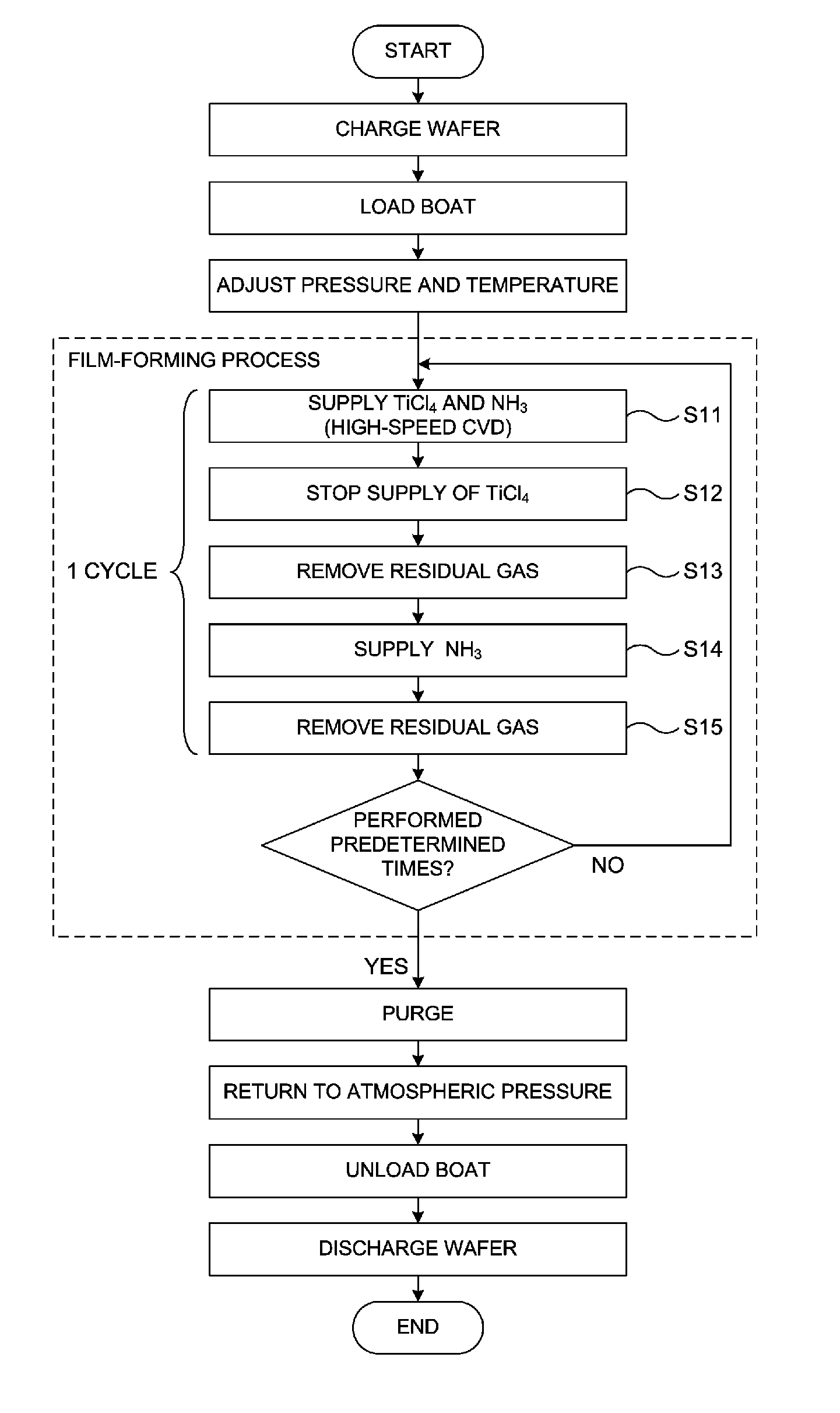
[0079]FIG. 4 illustrates a film-forming sequence of a TiN film according to a first embodiment. In addition, FIG. 5 is a flow diagram illustrating a process in accordance with the first embodiment.

[0080]In the film-forming process, the controller 280 controls the substrate processing apparatus 1 in a following manner. That is, the heater 207 maintains a temperature of the processing chamber 201 at which a CVD reaction occurs, for example, within a range of 250° C. to 800° C., preferably 700° C. or less, and more preferably 450° C. Thereafter, the plurality of wafers 200 are charged into the boat 217, and the boat 217 is loaded into the processing chamber 201. Subsequently, the boat 217 is rotated by the boat drive mechanism 267 to rotate the wafers 200. Thereafter, the valve 243 is opened and the vacuum pump 246 is operated to evacuate the inside of the processing chamber 201. When a temperature of the wafers 200 reaches 450° C. and the temperature is stabilized, a sequence to be de...

second embodiment

[0104]FIG. 6 shows a sequence according to a second embodiment. In addition, FIG. 7 is a flow diagram illustrating a process according to the second embodiment. The sequence according to the second embodiment will be described with reference to FIGS. 6 and 7.

[0105](Step S21)

[0106]In step S21, the valve 324 of the gas supply tube 320 is opened to supply the NH3 into the processing chamber 201. A time taken to expose the wafer 200 to the NH3 ranges, for example, from 0.1 to 30 seconds.

[0107](Step S22)

[0108]Next, the valve 314 of the gas supply tube 310 is opened to supply the TiCl4 into the processing chamber 201. A time taken to expose the wafer 200 to the TiCl4 and the NH3 ranges, for example, from 5 to 30 seconds.

[0109](Step S23)

[0110]In step S23, the valve 314 of the gas supply tube 310 is closed to stop the supply of the TiCl4 into the processing chamber 201, and the valve 614 is open to allow the TiCl4 to flow into the vent line 610. The supply of the TiCl4 into the processing c...

third embodiment

[0119]FIG. 8 shows a sequence according to a third embodiment. In addition, FIG. 9 is a flow diagram illustrating a process according to the third embodiment. Hereinafter the sequence according to the third embodiment will now be described with reference to FIGS. 8 and 9.

[0120](Step S31)

[0121]In step S31, the valve 314 of the gas supply tube 310 is opened to supply the TiCl4 into the processing chamber 201. A time taken to expose the wafer 200 to the TiCl4 ranges, for example, from 0.1 to 30 seconds.

[0122](Step S32)

[0123]Next, the valve 324 of the gas supply tube 320 is opened to supply the NH3 into the processing chamber 201. Here, A time period during which the wafer 200 is exposed to the TiCl4 and the NH3 ranges, for example, from 5 to 30 seconds.

[0124](Step S33)

[0125]In step S33, the valve 314 of the gas supply tube 310 is closed to stop the supply of the TiCl4 into the processing chamber 201, and the valve 614 is open to allow the TiCl4 to flow into the vent line 610. The suppl...


PUM

PropertyMeasurementUnit
temperatureaaaaaaaaaa

Abstract

A method of manufacturing a semiconductor device and a substrate processing apparatus capable of providing a TiN film that is higher in quality than a TiN film formed by a conventional CVD method at a higher film-forming rate, that is, with a higher productivity than a TiN film formed by an ALD method. The method includes steps of: (a) loading a substrate into a processing chamber; (b) forming a predetermined film on the substrate by simultaneously supplying the first processing gas and the second processing gas into the processing chamber; (c) stopping the supply of the first processing gas and the second processing gas and removing the first processing gas and the second processing gas remaining in the processing chamber; (d) modifying the film formed on the substrate by supplying the second processing gas into the processing chamber after the step (c); and (e) unloading the substrate from the processing chamber, wherein, in the step (b), a time period for supplying the second processing gas into the processing chamber is longer than a time period for supplying the first processing gas into the processing chamber.

Description

CROSS-REFERENCE TO RELATED PATENT APPLICATION[0001]This application claims priority to and the benefit of Japanese Patent Application Nos. 2010-013014 filed on Jan. 25, 2010 and 2010-266422 filed on Nov. 30, 2010 the disclosure of which is incorporated herein by reference.1. FIELD OF THE INVENTION[0002]The present invention relates to a method of manufacturing a semiconductor device and a substrate processing apparatus, and more particularly, to a method of manufacturing a semiconductor device and a substrate processing apparatus wherein a metal film or a metal compound is formed on a substrate (a wafer) using a halogenated metal compound or an organometallic compound as a source.2. DESCRIPTION OF THE RELATED ART[0003]Methods of forming a predetermined film on a substrate include a chemical vapor deposition (CVD) method. The CVD method is a method of forming a film including elements included in source molecules as components on a substrate using a reaction of at least two sources i...

Claims


Application Information

Patent Timeline
Patent Type & Authority Applications(United States)
IPC IPC(8): H01L21/3205C23C16/52C23C16/455
CPCC23C16/34C23C16/45523H01L21/32051H01L21/28556H01L21/28562C23C16/45574H01L21/205
Inventor KAGA, YUKINAOSAITO, TATSUYUKISAKAI, MASANORIYOKOGAWA, TAKASHI
Owner KOKUSA ELECTRIC CO LTD
Why Eureka
Try Eureka