
Low mismatch semiconductor device and method for fabricating same

a technology of low mismatch and semiconductor devices, applied in the field of semiconductor devices, can solve the problems of incompatibility of long channels as a solution to analog device mismatch and the trend towards ever-reduced device dimensions

Active Publication Date: 2011-08-04
AVAGO TECH INT SALES PTE LTD
View PDF2 Cites 6 Cited by
  • Summary
  • Abstract
  • Description
  • Claims
  • Application Information

AI Technical Summary

Benefits of technology

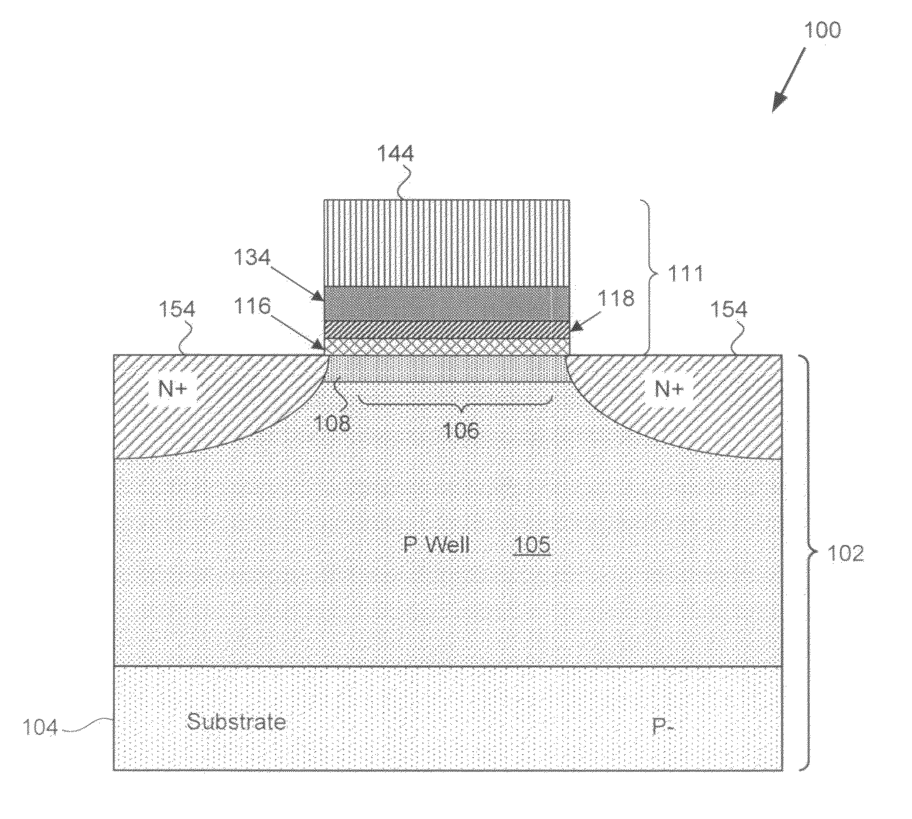
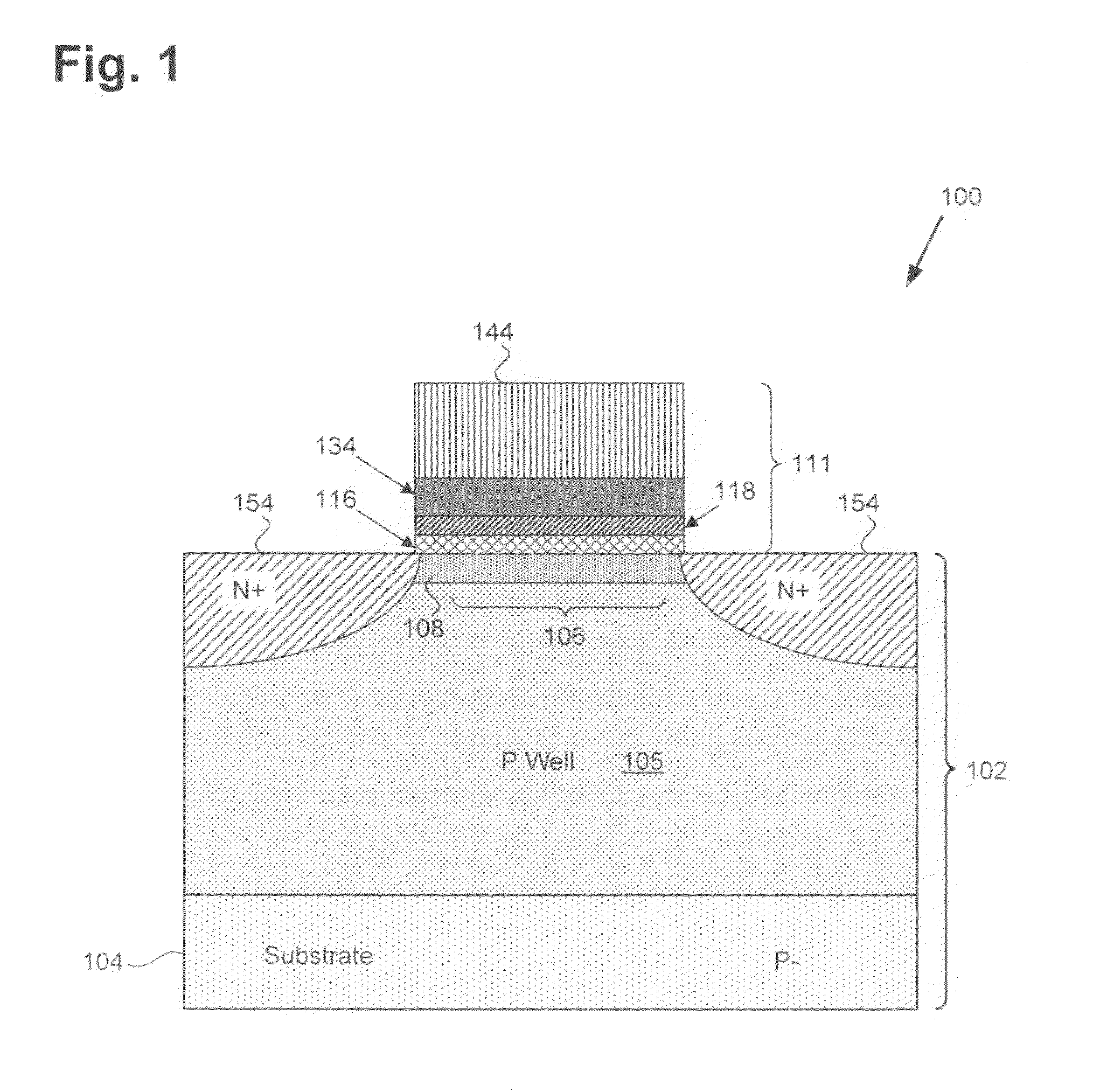
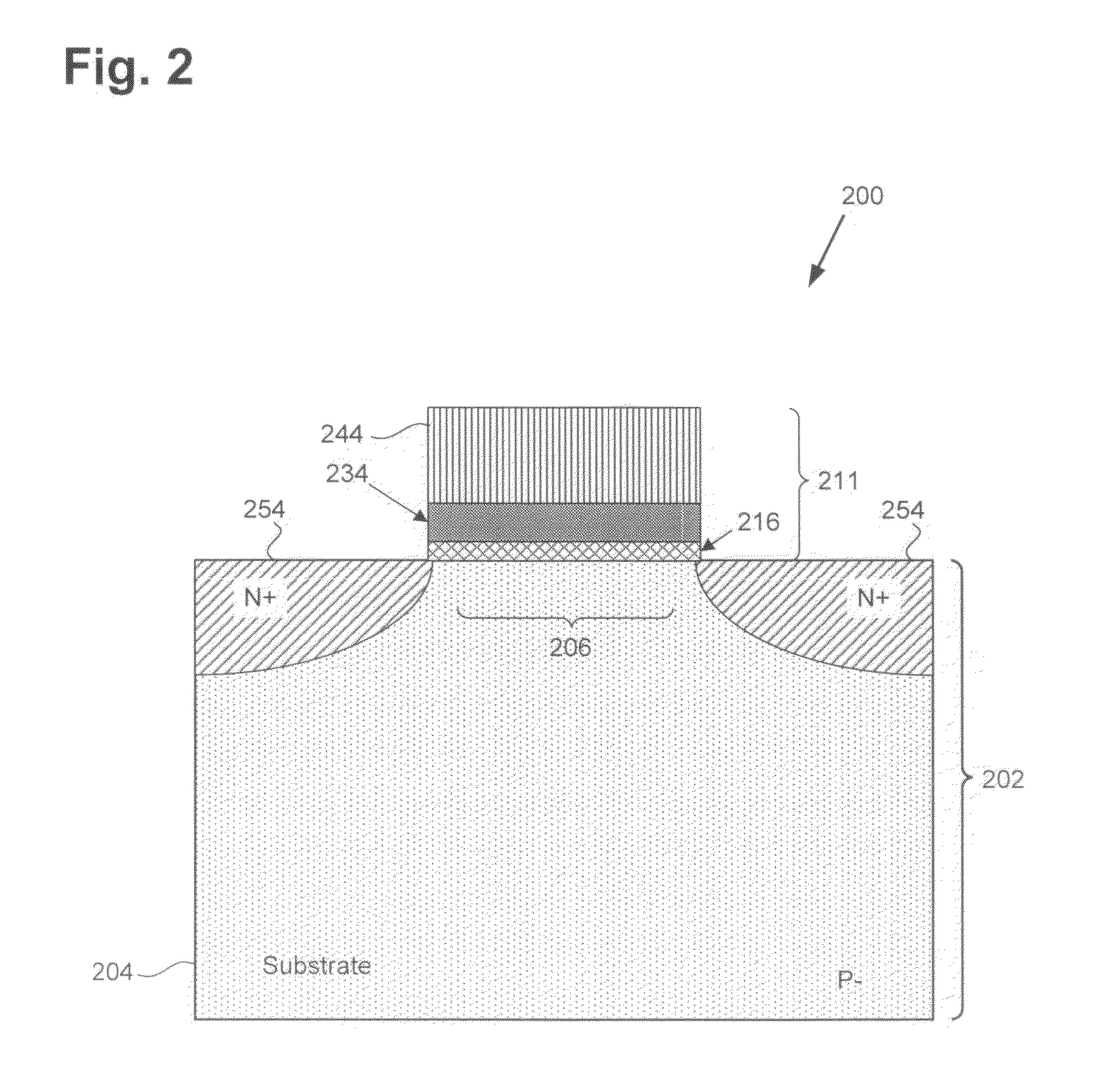
[0007]A low mismatch semiconductor device and method for fabricating same, substantially as shown in and / or described in connection with at least one of the figures, as set forth more completely in the claims.

Problems solved by technology

Mismatch is particularly critical to analog device performance.
However, the use of long channels as a solution to analog device mismatch is incompatible with the progressive advancement of process technologies towards ever reduced device dimensions.

Method used


Image

  • Low mismatch semiconductor device and method for fabricating same
  • Low mismatch semiconductor device and method for fabricating same
  • Low mismatch semiconductor device and method for fabricating same

Examples


Embodiment Construction

[0016]The present invention is directed to a low mismatch semiconductor device and method for its fabrication. Although the invention is described with respect to specific embodiments, the principles of the invention, as defined by the claims appended herein, can obviously be applied beyond the specifically described embodiments of the invention described herein. Moreover, in the description of the present invention, certain details have been left out in order to not obscure the inventive aspects of the invention. The details left out are within the knowledge of a person of ordinary skill in the art.

[0017]The drawings in the present application and their accompanying detailed description are directed to merely example embodiments of the invention. To maintain brevity, other embodiments of the invention, which use the principles of the present invention, are not specifically described in the present application and are not specifically illustrated by the present drawings. It should b...


PUM


Abstract

Disclosed is a low mismatch semiconductor device that comprises a lightly doped channel region having a first conductivity type and a first dopant concentration in a semiconductor body, and a high-k metal gate stack including a gate metal layer formed over a high-k gate dielectric without having a dielectric cap on the high-k dielectric. The high-k metal gate stack being formed over the lightly doped channel region. The lightly doped channel region may be a P- or N-conductivity region, for example, and may be part of a corresponding P- or N-semiconductor substrate, or a P- or N-well formed in a substrate of the respectively opposite conductivity type. The disclosed semiconductor device, which may be an NMOS or PMOS analog device, for example, can be fabricated as part of an integrated circuit including one or more CMOS logic devices.

Description

BACKGROUND OF THE INVENTION[0001]1. Field of the Invention[0002]The present invention is generally in the field of semiconductors. More specifically, the present invention is in the field of fabrication of semiconductor devices.[0003]2. Background Art[0004]Due to its numerous advantages, such as high density, low power consumption, and relative noise immunity, for example, complementary metal-oxide-semiconductor (CMOS) technology is widely used in control logic circuits, and in analog circuits implemented as part of the integrated circuits (ICs) used in modern electronic systems. As advancements in process technologies have resulted in CMOS devices being scaled down, and their operating voltages correspondingly reduced, device features have evolved to include, for example, high dielectric constant (high-k) metal gate designs.[0005]Mismatch is particularly critical to analog device performance. A conventional fabrication strategy responsive to the problem of mismatch employs the use ...

Claims


Application Information

Patent Timeline
Patent Type & Authority Applications(United States)
IPC IPC(8): H01L27/092H01L29/78H01L21/28
CPCH01L21/28H01L27/092H01L29/78H01L21/823842H01L21/823857H01L29/517H01L29/4966H01L29/7833H01L21/28088H01L29/6659H01L29/513
Inventor CHEN, XIANGDONGITO, AKIRA
Owner AVAGO TECH INT SALES PTE LTD
Learn More