Solid-state imaging device and driving method thereof

a solid-state imaging and driving method technology, applied in the direction of semiconductor devices, radio frequency controlled devices, electrical devices, etc., can solve the problems of degrading charge transfer efficiency, achieve the effect of improving charge transfer efficiency, suppressing the generation of dark current, and improving charge transfer efficiency

Inactive Publication Date: 2011-08-11
RENESAS ELECTRONICS CORP
View PDF0 Cites 8 Cited by
  • Summary
  • Abstract
  • Description
  • Claims
  • Application Information

AI Technical Summary

Benefits of technology

[0018]According to the present invention, in the solid-state imaging device, it is possible to provide a technique for improving charge transfer efficiency while suppressing generation of the dark current.
[0019]Each of regions under charge storage gate electrodes has a different impurity concentration, and a voltage setting range is defined to allow pinning in the entire region, whereby the charge transfer efficie

Problems solved by technology

The extension of the charge storage section ca

Method used


Image

  • Solid-state imaging device and driving method thereof
  • Solid-state imaging device and driving method thereof
  • Solid-state imaging device and driving method thereof

Examples


first embodiment

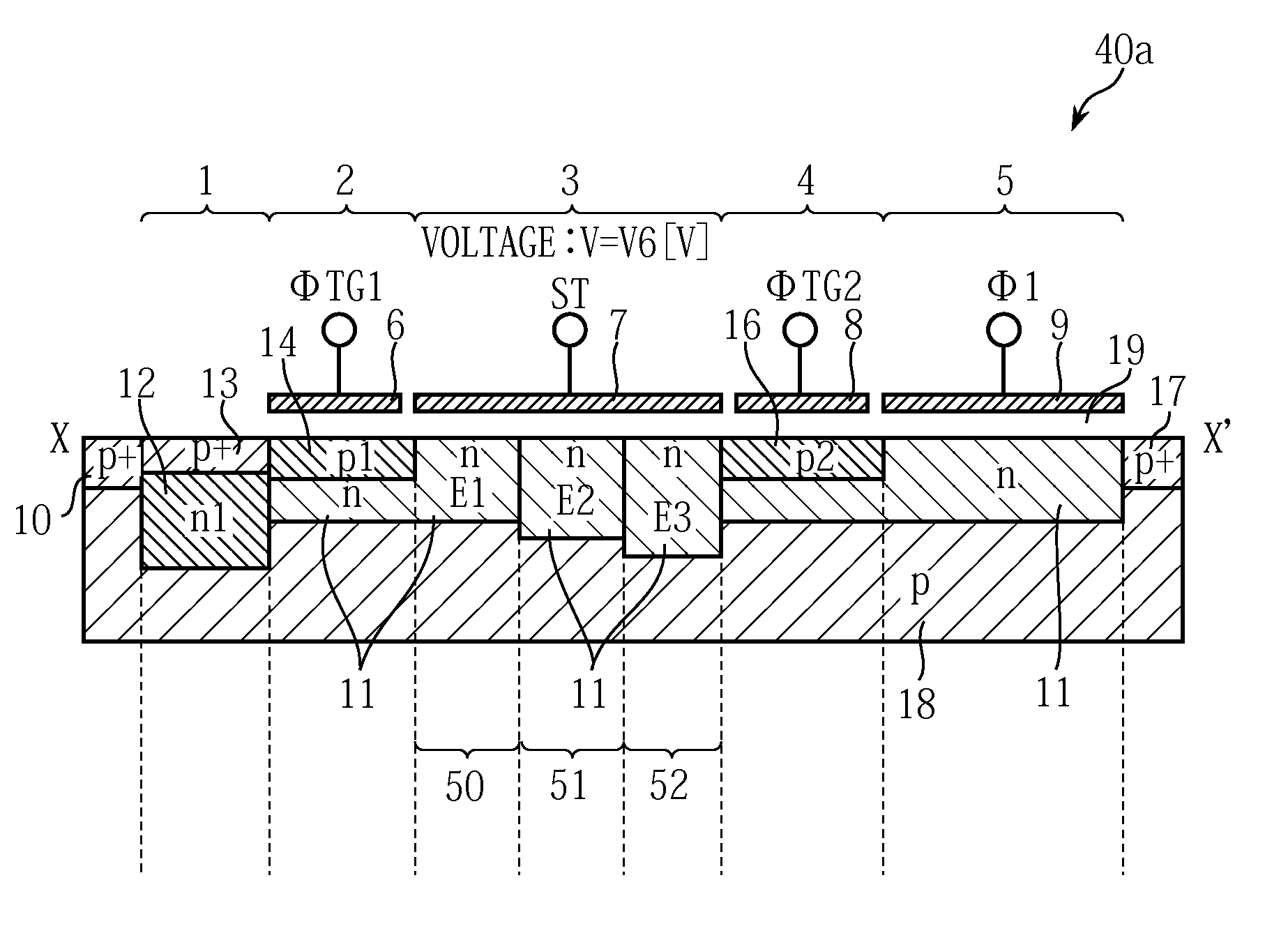
[0074]The solid-state imaging device 40 has a photoelectric conversion section (or photodiode) 1 including an n-type diffusion layer 12 with the impurity concentration of n1, a charge transfer gate section 2 including a charge transfer gate electrode 6, a charge storage section 3 including a charge storage gate electrode 7, a charge transfer gate section 4 including a charge transfer gate electrode 8, and a CCD section 5 including a CCD region 21. In the solid-state imaging device 40, the charge transfer gate section 2 is interposed between the photoelectric conversion section (e.g. photodiode) 1 and the charge storage section 3. The charge transfer gate section 4 is interposed between the charge storage section 3 and the CCD section 5. The CCD section 5 is provided with a set of a CCD section gate electrode 9, a CCD section gate electrode 20, a CCD section gate electrode 25, and a CCD section gate electrode 26 for a change transfer row, and an output amplifier 22 is arranged in one...

second embodiment

[0112]A second embodiment of the present invention will be described below. FIG. 15A shows a cross section of the solid-state imaging device 40 according to the second embodiment. FIG. 15B shows a transition state of potential wells in the cross section. A solid line and a broken line in FIG. 15B show a potential transition state in response to a voltage applied to each of the electrodes. It should be noted that a plan view of the solid-state imaging device 40 according to the second embodiment is the same as that of the first embodiment. As shown in FIG. 15A, the solid-state imaging device 40 according to the second embodiment has three regions under the charge storage gate electrode 7: the n-type diffusion layer 11 with the impurity concentration of n, the n-type diffusion layer 15 with the impurity concentration of n2 and an n-type diffusion layer 15a with the impurity concentration of n3. The n-type diffusion layer 11 is the region with the impurity concentration of n. The n-typ...

third embodiment

[0123]A third embodiment of the present invention will be described below. FIG. 17A shows a cross section of the solid-state imaging device 40 according to the third embodiment. FIG. 17B shows a transition state of potential wells in the cross section. A solid line and a broken line in FIG. 17B show a potential transition state in response to a voltage applied to each of the electrodes. It should be noted that a plan view of the solid-state imaging device 40 according to the third embodiment is the same as that of the first embodiment or the second embodiment. As shown in FIG. 17A, in the solid-state imaging device 40 according to the third embodiment, two regions of an n-type diffusion layer 15b with the impurity concentration of n4 and an n-type diffusion layer 15c with the impurity concentration of n5 are formed under the charge storage gate electrode 7. It is assumed that the following condition is satisfied between the impurity concentration of n4 and the impurity concentration...


PUM


Abstract

A solid-state imaging device includes: a photoelectric converting section comprising a photo-diode; a charge storage section; a charge transfer section; a first control gate section provided between the photoelectric converting section and the charge storage section to control transfer of a signal charge from the photoelectric converting section to the charge storage section; and a second control gate section provided between the charge storage section and the charge transfer section to control transfer of the signal charge from the charge storage section to the charge transfer section. The charge storage section includes: a first region formed on a side near to the first control gate section; and a second region formed on a side near to the second control gate section and configured to have a channel potential increased more than that of the first region. The second region is configured to hold the signal charge in a pinning condition.

Description

INCORPORATION BY REFERENCE[0001]This patent application claims priorities on convention based on Japanese Patent Application No. 2010-26885 filed on Feb. 9, 2010 and Japanese Patent Application No. 2010-198571 filed on Sep. 6, 2010. The disclosures thereof are incorporated herein by reference.TECHNICAL FIELD [0002]The present invention relates to a solid-state imaging device and a driving method thereof.BACKGROUND ART[0003]In one of structures of solid-state imaging devices, a charge storage section (or memory) is interposed between a photodiode and a CCD section to temporarily store charges. In an image sensor provided with the charge storage section, since a dark current increases in proportion to a time period for which the charges are held in the charge storage section, image degradation becomes more remarkable in a case of storing the charges for a longer time period. Also, the dark current is almost doubled in the temperature rise by 8 to 10° C. Because of the above reasons, i...

Claims


Application Information

Patent Timeline
IPC IPC(8): H01L27/148
CPCH01L29/76816H01L27/14812
Inventor GOTO, RYOICHI
Owner RENESAS ELECTRONICS CORP
Why Eureka
Try Eureka