Semiconductor integrated circuit for driving display panel, display panel driving module, and display device

Inactive Publication Date: 2011-08-18
PANASONIC SEMICON SOLUTIONS CO LTD
View PDF19 Cites 3 Cited by
  • Summary
  • Abstract
  • Description
  • Claims
  • Application Information

AI Technical Summary

Benefits of technology

[0067]The present invention can succeed in controlling an area increase of wiring and diffusion regions, which was conventionally infeasible, so that reduction of a chip area is accomplished, while guaranteeing a good testing facility for checking whether gradation wiring lines are short-circuited due to any failure in a semiconductor manufacturing process.

Problems solved by technology

The ongoing trend, however, structurally complicates a semiconductor integrated circuit configured to drive the display panel, making a test analysis difficult.
Therefore, there is the risk of short circuit between the gradation wiring lines due to any failure in a semiconductor manufacturing process.
When the potential is applied to two terminals as illustrated in FIG. 9, there is a constant current flow, which makes it difficult to determine whether the current results from the short circuit between the gradation wiring lines.
When the current leakage is thus checked by simply applying the potential, it is difficult to decide whether the gradation wiring lines are short-circuited, leading to an increase of testing steps.
Thus, it is inconvenient to test whether the gradation wiring lines are short-circuited in the prior art 1 illustrated in FIGS. 6 and 7.

Method used


Image

  • Semiconductor integrated circuit for driving display panel, display panel driving module, and display device
  • Semiconductor integrated circuit for driving display panel, display panel driving module, and display device
  • Semiconductor integrated circuit for driving display panel, display panel driving module, and display device

Examples


exemplary embodiment 1

[0079]In exemplary embodiments 1 and 2 of the present invention described below (and in the Scope of Claims), n, n′, m, m′, and p are all positive integer numbers, and such ordinal numbers as (n) th and (n+1)th express an arrangement order of equivalent elements disposed in juxtaposition. Further, (n) th and (n+1)th, and (n−1)th and (n) th respectively express that the elements with these prefix numbers are adjacent to each other in the arrangement order.

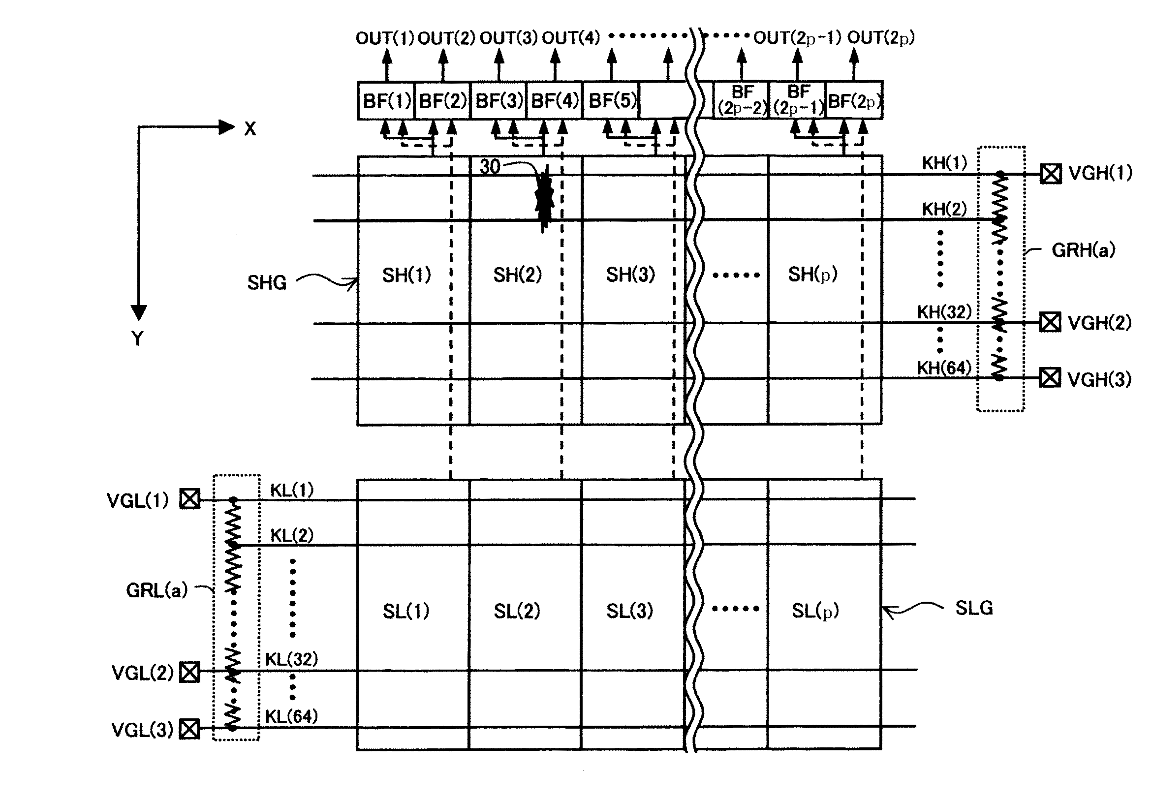
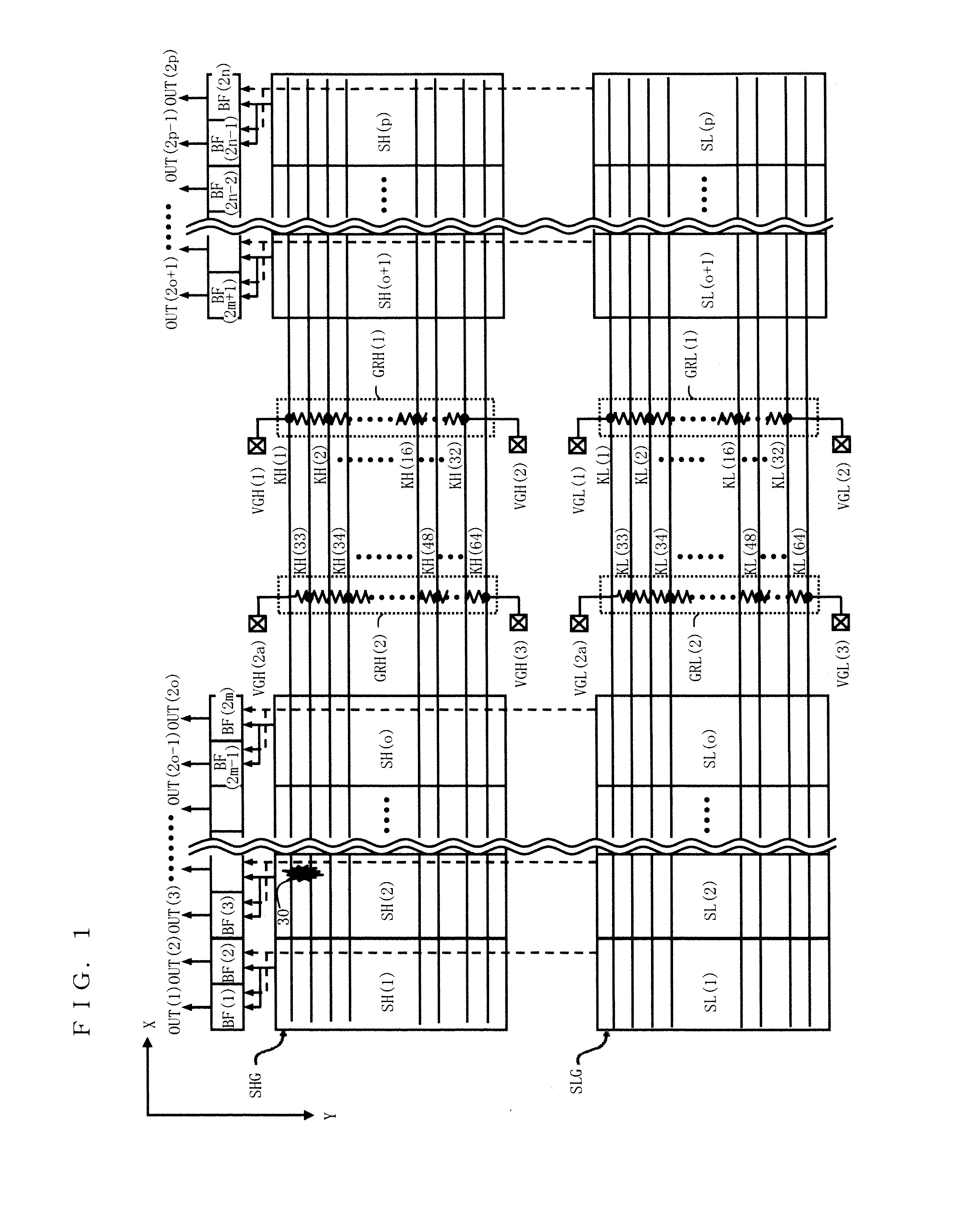
[0080]A semiconductor integrated circuit for display panel drive according to the exemplary embodiments is adapted to dot inversion driving, wherein there are three gradation reference potential inputs on positive and negative polarities respectively, and the display gradation of a liquid crystal panel is 64 gradation levels during normal use, but four gradation reference potential inputs are used on the positive and negative polarities to test whether any gradation wiring lines are short-circuited.

[0081]FIGS. 1 and 3 are circuit di...

exemplary embodiment 2

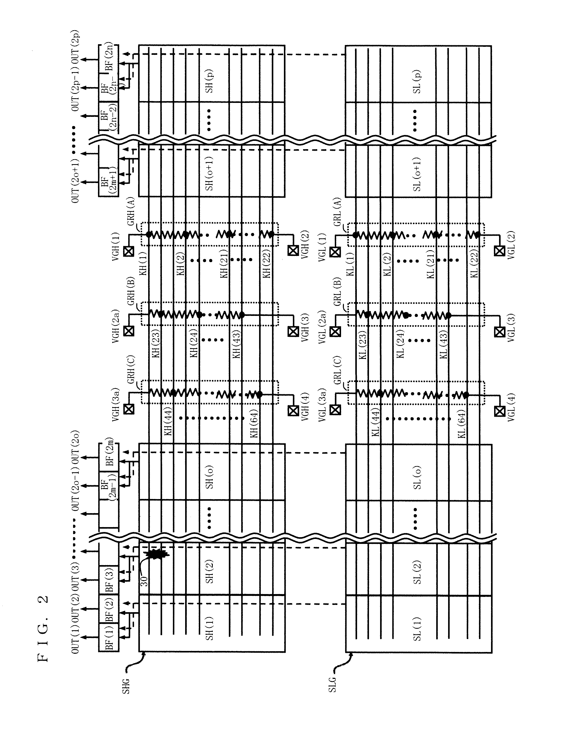
[0106]Before an exemplary embodiment 2 of the present invention is described, a technical object to be achieved by the exemplary embodiment 2 is described referring to FIG. 11. FIG. 11 is a circuit diagram of a comparative example to the exemplary embodiment 2, conceptually illustrating a main section of a display panel driving module or a display device. Referring to FIG. 11, 10 is a semiconductor integrated circuit for display panel drive, and 20 is a package to which the gradation potentials are inputted. The gradation potentials are applied from an external connection terminal Vrf (k) to an electrode pad VGH (k), and the gradation potentials are then supplied to the semiconductor integrated circuit 10 for display panel drive (k=1, 2, 3). Because of a structure normally provided wherein the external connecter terminal Vrf and the electrode pad are equally provided, it is a difficult task to accomplish the solution of the inter-wiring short circuit test on the package 20. Accordin...


PUM


Abstract

Gradation wiring lines of positive polarity included in a (m)th group of wiring lines of positive polarity and gradation wiring lines of positive polarity included in a (m+1)th group of wiring lines of positive polarity are alternately provided. Gradation wiring lines of negative polarity included in a (m′)th group of wiring lines of negative polarity and gradation wiring lines of negative polarity included in a (m′+1)th group of wiring lines of negative polarity are alternately provided. First −(n) th resistance dividing circuits of positive polarity include (m)th resistance dividing circuits of positive polarity provided between the gradation wiring lines of positive polarity or on one end side of a direction where the gradation wiring lines of positive polarity extend and connected to the (m)th group of wiring lines of positive polarity, and (m+1)th resistance dividing circuits of positive polarity provided between the gradation wiring lines of positive polarity or on the other end side of the direction where the gradation wiring lines of positive polarity extend and connected to the (m+1)th group of wiring lines of positive polarity. First −(n′)th resistance dividing circuits of negative polarity include (m′)th resistance dividing circuits of negative polarity provided between the gradation wiring lines of negative polarity or on one end side of a direction where the gradation wiring lines of negative polarity extend and connected to the (m′)th group of wiring lines of negative polarity, and (m′+1)th resistance dividing circuits of negative polarity provided between the gradation wiring lines of negative polarity or on the other end side of the direction where the gradation wiring lines of negative polarity extend and connected to the (m′+1)th group of wiring lines of negative polarity.

Description

FIELD OF THE INVENTION[0001]The present invention relates to a semiconductor integrated circuit configured to drive a display panel such as a liquid crystal display panel, more particularly to a technology mostly developed for a semiconductor integrated circuit adapted to dot inversion driving and capable of reducing a chip area while guaranteeing a good testing facility for testing whether short circuit is occurring between gradation wiring lines due to any failure in a semiconductor manufacturing process. The present invention further relates to a display panel driving module and a display device configured likewise.BACKGROUND OF THE INVENTION[0002]In recent years, there is an ongoing reduction of frame width in display panels used for OA (Office Automation). More specifically, a frame member circumferentially encompassing a cabinet which holds a display panel body has an increasingly narrower width. Conventionally, signal wiring lines are provided in the frame member having a lar...

Claims


Application Information

Patent Timeline
IPC IPC(8): G09G5/10
CPCG02F2203/30G09G3/3696G09G3/3685G09G3/3614
Inventor IKEDA, HIDEKIDOI, YASUYUKI
Owner PANASONIC SEMICON SOLUTIONS CO LTD
Why Eureka
Try Eureka