Circuit board capable of loading high electrical current

a high-current, circuit board technology, applied in the direction of electrical apparatus contruction details, substation/switching arrangement casing, electrical components association, etc., can solve the problems of inefficient improvement of the manufacture efficiency of the printed circuit board, general relatively thin thickness of copper foil, and disadvantages of common commercially available printed circuit board manufacturing and operation, etc., to achieve convenient change and efficient simplified circuit board manufacturing process

a high-current, circuit board technology, applied in the direction of electrical apparatus contruction details, substation/switching arrangement casing, electrical components association, etc., can solve the problems of inefficient improvement of the manufacture efficiency of the printed circuit board, general relatively thin thickness of copper foil, and disadvantages of common commercially available printed circuit board manufacturing and operation, etc., to achieve convenient change and efficient simplified circuit board manufacturing process

US20110199743A1Inactive Publication Date: 2011-08-18CHEN TSAN CHI

Image

  • Circuit board capable of loading high electrical current
  • Circuit board capable of loading high electrical current
  • Circuit board capable of loading high electrical current

Examples


Embodiment Construction

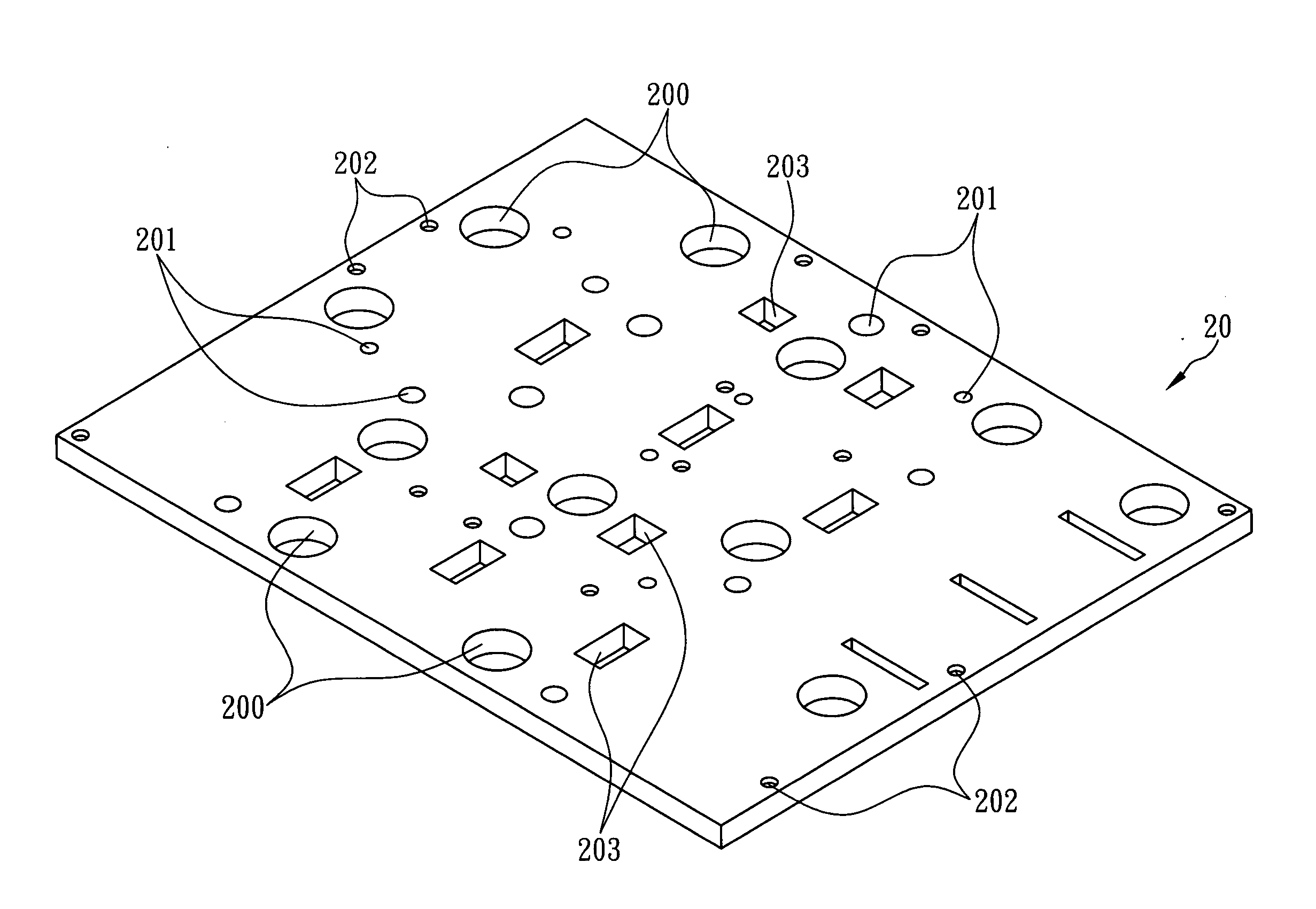
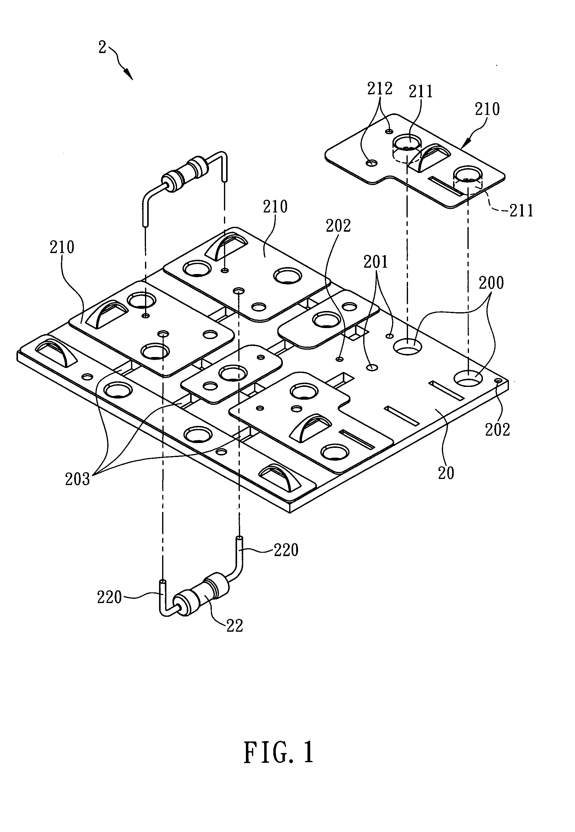
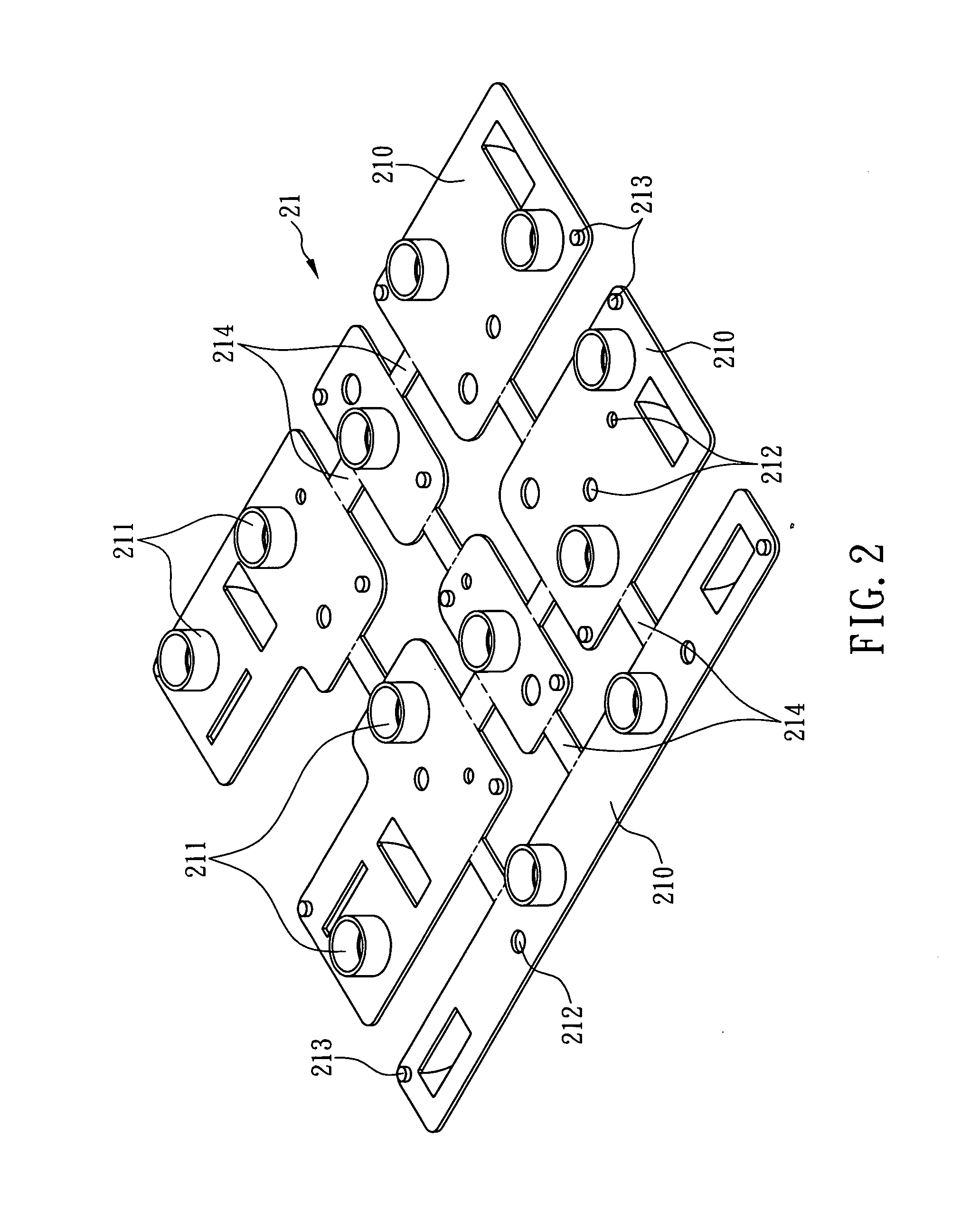
[0018]The present invention is related to a circuit board capable of loading high electrical current. Referring now to FIG. 1, a circuit board according to a preferred embodiment of the present invention is illustrated. As shown, the circuit board designated by numeral 2 comprises an insulation plate 20 and a plurality of conductive plates 210, wherein the insulation plate 20 is evenly formed with a plurality of first riveting portions 200 (such as riveting holes or riveting posts) and a plurality of first insertion holes 201. Each of the conductive plates 210 is formed by punching and cutting a metal plate 21 (as shown in FIG. 2), and each of the conductive plates 210 is formed with at least one second riveting portion 211 (such as riveting posts or riveting holes). Each of the second riveting portions 211 can be matched with each of the first riveting portions 200 to combine with each other, so that each of the conductive plates 210 can be positioned on the insulation plate 20 by ...


PUM


Abstract

The present invention is to provide a circuit board capable of loading high electrical current, which comprises an insulation plate and a plurality of conductive plates each positioned on the insulation plate by riveting. A plurality of first insertion holes of the insulation plate are aligned with a plurality of second insertion holes of the conductive plates, respectively, so that the aligned first and second insertion holes of the circuit board can be welded with a plurality of electric components (such as resistors, capacitors, fuses, etc.). Therefore, the insulation plate and each of the conductive plates can be easily combined with each other by riveting to form a finished product of the circuit board without some complicated steps including exposure, development and etching, so that the manufacturing process of the circuit board capable of loading high electrical current can be efficiently simplified.

Description

FIELD OF THE INVENTION[0001]The present invention relates to a circuit board, more particularly to a circuit board formed by riveting a plurality of conductive plates onto an insulation plate and capable of loading high electrical current.BACKGROUND OF THE INVENTION[0002]Nowadays, a printed circuit board (PCB) is an electronic component widely used in an electronic product of low current (such as a mobile phone, a digital camera, a PDA, a liquid crystal display, etc.) or an industrial apparatus of high electrical current (such as an electric control device, an electric transformation device, a cooling system, a multi-way socket, a socket of extension cord, etc.). According to the survey, there are still some disadvantages existing in the manufacture and operation of common commercially-available printed circuit boards. For example, a traditional photosensitive printed circuit board is described hereinafter, wherein a semi-finished product of the printed circuit board is provided wit...

Claims


Application Information

Patent Timeline
18 Aug 2011
Publication
US20110199743A1
IPC
H05K1/18
CPC
H05K1/0263; H05K3/202; H05K2203/167; H05K2201/10401; H05K3/306
Inventors
CHEN, TSAN-CHI