Growth of multi-junction LED film stacks with multi-chambered epitaxy system

a technology of led film and epitaxy system, which is applied in the direction of semiconductor/solid-state device manufacturing, electrical equipment, semiconductor/solid-state device manufacturing, etc., can solve the problems of cross-contamination between different layers, severe parasitic coating of process, and delay in turn-on and turn-off of dopants

Inactive Publication Date: 2011-08-25
APPLIED MATERIALS INC
View PDF15 Cites 134 Cited by
  • Summary
  • Abstract
  • Description
  • Claims
  • Application Information

AI Technical Summary

Benefits of technology

[0039]In an embodiment, a Mg-free film layer is grown after a Mg-doped film layer is grown over a substrate with an abrupt Mg profile there between. In one such embodiment, a p-type layer film (e.g., pGaN) doped with Mg is grown in a first epitaxial chamber of a multi-chambered epitaxy system and a non-p-type-doped film (e.g., nGaN) substantially free of Mg is grown over the Mg-doped film layer in a second epitaxial chamber of the multi-chambered

Problems solved by technology

Due to the complex metal-organic precursors, the deposition process is accompanied with severe parasitic coatings, c

Method used


Image

  • Growth of multi-junction LED film stacks with multi-chambered epitaxy system
  • Growth of multi-junction LED film stacks with multi-chambered epitaxy system
  • Growth of multi-junction LED film stacks with multi-chambered epitaxy system

Examples


Embodiment Construction

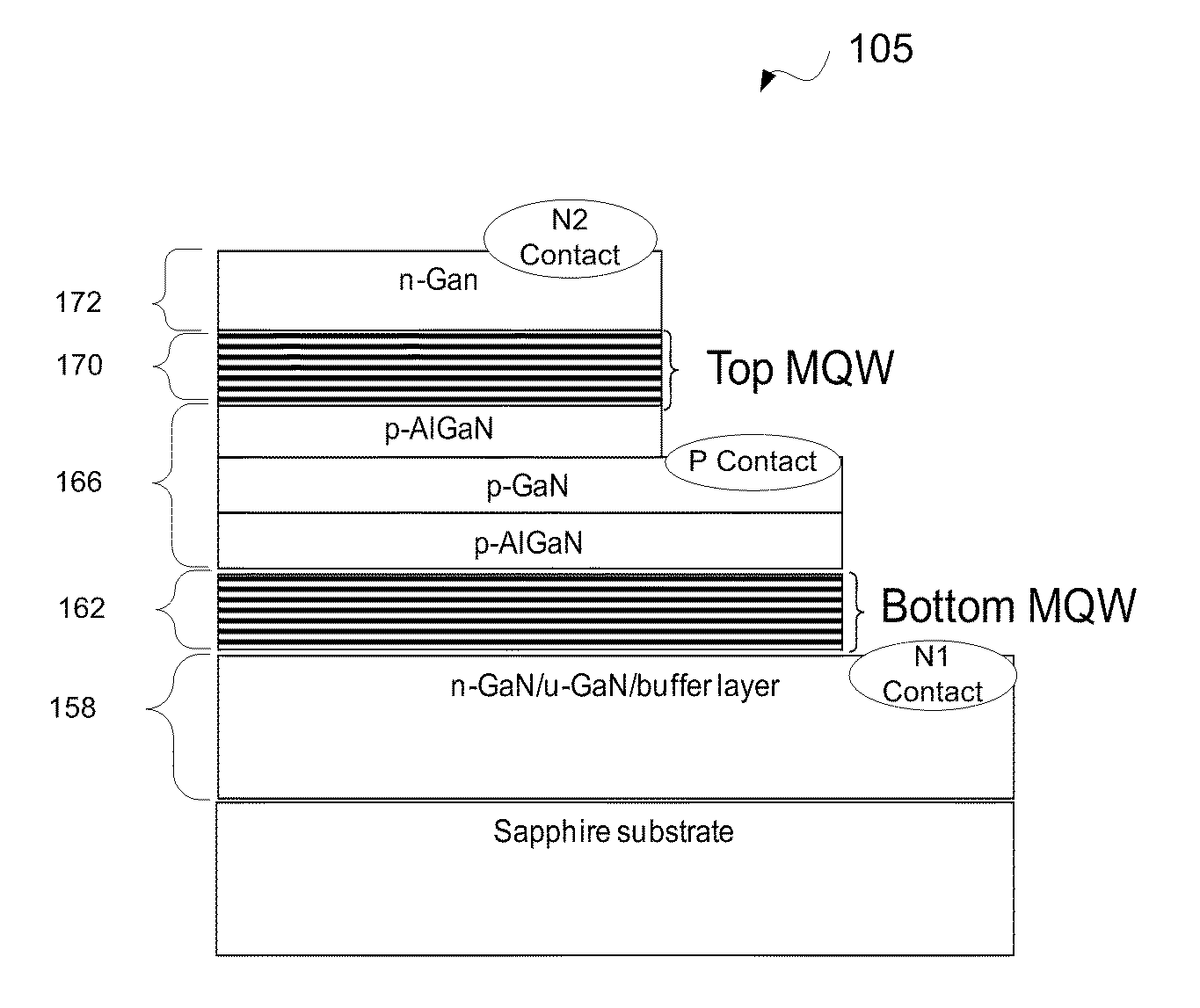
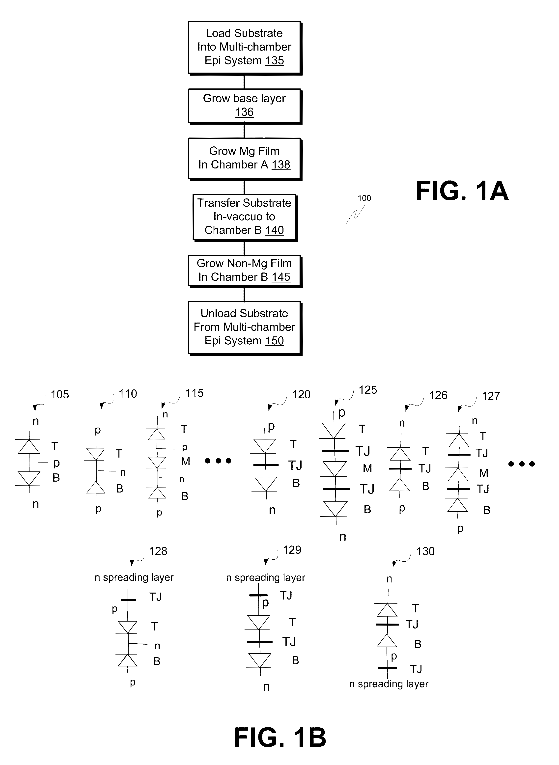
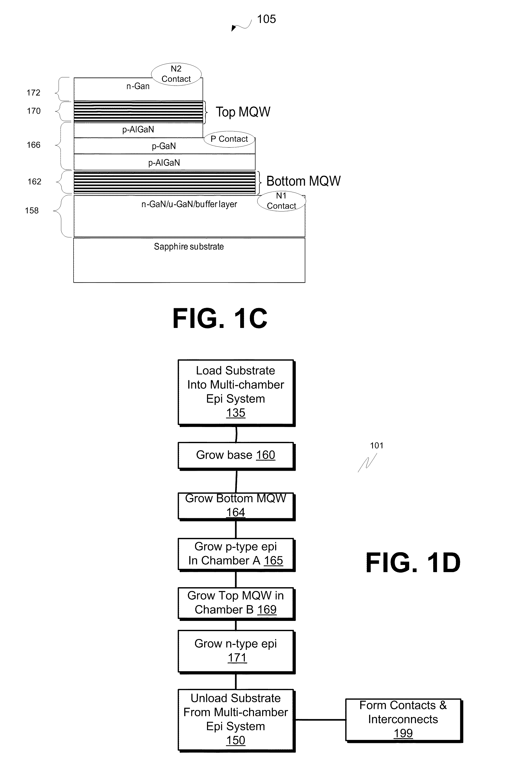
[0043]In the following description, numerous details are set forth. It will be apparent, however, to one skilled in the art, that the present invention may be practiced without these specific details. In some instances, well-known methods and devices are shown in block diagram form, rather than in detail, to avoid obscuring the present invention. Reference throughout this specification to “an embodiment” means that a particular feature, structure, function, or characteristic described in connection with the embodiment is included in at least one embodiment of the invention. Thus, the appearances of the phrase “in an embodiment” in various places throughout this specification are not necessarily referring to the same embodiment of the invention. Furthermore, the particular features, structures, functions, or characteristics may be combined in any suitable manner in one or more embodiments. For example, a first embodiment may be combined with a second embodiment anywhere the two embod...


PUM


Abstract

Apparatus and method for growth of non-p-type GaN layers over p-type GaN layers. Embodiments include multi-junction LED film stacks, multi-junction LED devices paired into units and multi-junction LED arrays of the paired units. Epitaxial growths of p-type and non-p-type material layers are split between epitaxial chambers clustered onto a single platform to reduce p-type dopant cross-contamination. Arrayed multi-junction LED devices provide improved packing density and reduced blinking during AC operation.

Description

CLAIM OF PRIORITY[0001]This application is related to, and claims priority to, the provisional utility application entitled “GROWTH OF MULTI-JUNCTION LED FILM STACKS WITH MULTI-CHAMBERED EPITAXY SYSTEM,” filed on Feb. 23, 2010, having an application No. 61 / 307,192 and attorney docket no. 014490L / ALRT / EES / NEON / ESONG.BACKGROUND[0002]1. Field[0003]Embodiments of the present invention pertain to the field of light-emitting diode (LED) fabrication and, in particular, to growth of multi-junction LED film stacks.[0004]2. Description of Related Art[0005]Group III-V materials are playing an ever increasing role in the semiconductor and related, e.g. light-emitting diode (LED), industries. Often, group III-V materials are difficult to grow or deposit in succession to form a film stack including a plurality of both n-type and p-type layers. Conventional III-V materials-based LED structures include only a single junction, which is typically grown in a single chamber without growth interruption....

Claims


Application Information

Patent Timeline
IPC IPC(8): H01L33/30H01L21/20
CPCH01L21/0242H01L21/02458H01L21/02507H01L21/0254H01L33/0016H01L27/156H01L33/007H01L33/08H01L25/0756H01L2224/48137H01L2924/0002
Inventor SU, JIEBOUR, DAVID
Owner APPLIED MATERIALS INC
Why Eureka
Try Eureka