

Semiconductor device and manufacturing method thereof
Active Publication Date: 2011-08-25
RENESAS ELECTRONICS CORP
View PDF14 Cites 38 Cited by
- Summary
- Abstract
- Description
- Claims
- Application Information
AI Technical Summary
Benefits of technology
[0011]According to the present invention, while the metal cap film is provided in the gate insulating film of the logic region, the RAM region does not have the metal cap film. As a result, it is possible to control the threshold voltage without implanting excessive ions to the RAM region. In addition, the RAM region may be formed as a structure that does not have difficulty in the process. Therefore, it is possible to reduce variability in the threshold voltage of the RAM region, and obtain an embedded memory device with an excellent product yield.
[0012]According to the present invention, it is possible to reduce variability in the threshold voltage of the RAM region and obtain an embedded memory device with an excellent product yield.
Problems solved by technology
When the memory and the logic circuit are integrated using the HK / MG process, it is problematic that allowable limits of the leakage currents in each region are different.
However, the inventor found the following problem.
In addition, since a random variability of the transistor characteristics is increased, and an abnormal leakage current becomes easy to occur, particularly, the product yield of the embedded SRAM device may be degraded.
Method used
View moreImage
Smart ImageViewing Examples

Examples
reference example 1
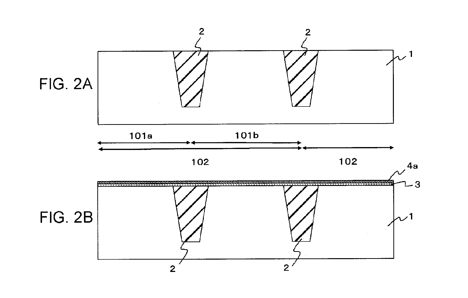
[0058]In the structure of the example, LaOx was formed in the NMOS transistor of the DRAM region 102. Lanthanum (La) was prepared by changing the thickness of 0.1 nm to 0.4 nm.
reference example 2
[0059]In the structure of the example, LaOx was formed in the NMOS transistor of the DRAM region 102. However, boron (B) ions at 3.8×1013 cm−3 were implanted to the NMOS region 102 of the silicon substrate 1 such that the threshold voltage Vth of the transistor 40 became 0.5 V.
Login to View More PUM
 Abstract
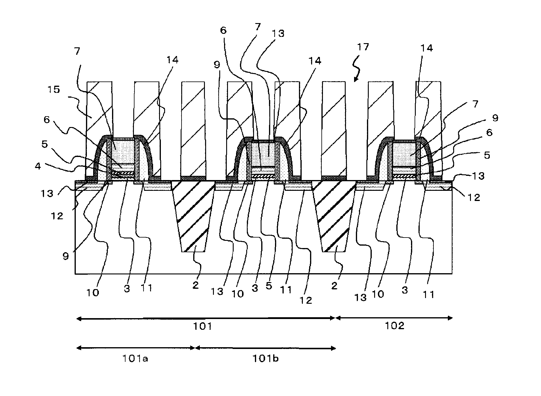
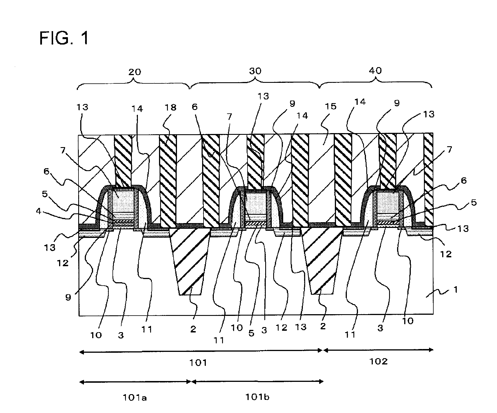
The semiconductor device of the present invention includes a silicon substrate having a logic region and a RAM region, an NMOS transistor formed in the logic region, and an NMOS transistor formed in the RAM region. The NMOS transistor has a stack structure obtained by sequentially stacking the gate insulating film and the metal gate electrode over the silicon substrate. The NMOS transistor has a cap metal containing an element selected from a group consisting of lanthanum, ytterbium, magnesium, strontium, and erbium as a composition element between the silicon substrate and metal gate electrode. The cap metal is not formed in the NMOS transistor.
Description
[0001]This application is based on Japanese patent application No. 2010-039768, the content of which is incorporated hereinto by reference.BACKGROUND[0002]1. Technical Field[0003]The present invention relates to a semiconductor device and a manufacturing method thereof.[0004]2. Related Art[0005]Recently, in advanced device development for miniaturization after 32 nm node generation, it is anticipated that a high-dielectric constant (high-k) gate insulating film / metal gate (HK / MG) process technique will be put into practical use. In addition, there is known a technique, in which a memory such as a dynamic random access memory (DRAM), a static random access memory (SRAM) and a logic circuit such as a complementary metal oxide semiconductor (CMOS) are integrated on the same substrate. When the memory and the logic circuit are integrated using the HK / MG process, it is problematic that allowable limits of the leakage currents in each region are different.[0006]Japanese Laid-open Patent P...
Claims
Login to View More Application Information
Patent Timeline
 IPC IPC(8): H01L27/092H01L21/28
CPCH01L21/28194H01L21/823462H01L2924/0002H01L21/823857H01L27/092H01L27/10873H01L27/10894H01L29/4966H01L29/513H01L29/517H01L29/6656H01L29/6659H01L29/7833H01L2924/00H10B12/05H10B12/09
InventorMORIYA, TOMOHIKO
OwnerRENESAS ELECTRONICS CORP