Manufacturing method for a solid-state image pickup device

a solid-state image and manufacturing method technology, applied in semiconductor/solid-state device manufacturing, semiconductor devices, electrical devices, etc., can solve the problems of difficult handling, difficult to adopt a complicated process for forming a large number of spacers, and lower rigidity of glass substrates

Inactive Publication Date: 2011-08-25
FUJIFILM CORP
View PDF5 Cites 20 Cited by
  • Summary
  • Abstract
  • Description
  • Claims
  • Application Information

AI Technical Summary

Benefits of technology

[0018]According to the presently disclosed subject matter, it is possible to stably manufacture a high-quality thin-type solid-state image pickup device at the wafer level.

Problems solved by technology

On the other hand, in the case where a thin-type solid-state image pickup device is manufactured at the wafer level as described above, the following problem arises.
However, the rigidity of the glass substrate becomes lower as the glass substrate is made thinner.
Therefore, the glass substrate sags under its own weight, and becomes prone to breakage state, which leads to difficult handling.
It is extremely difficult to adopt a complicated process for forming a large number of spacers with the use of the thin glass substrate having a reduced rigidity.

Method used


Image

  • Manufacturing method for a solid-state image pickup device
  • Manufacturing method for a solid-state image pickup device
  • Manufacturing method for a solid-state image pickup device

Examples


Embodiment Construction

[0022]Hereinafter, a preferred embodiment of the presently disclosed subject matter is described with reference to the accompanying drawings. Although the presently disclosed subject matter is described by way of the following preferred embodiment, the presently disclosed subject matter can be changed according to various methods without departing from the scope of the presently disclosed subject matter, and embodiments other than the present embodiment can be adopted. Accordingly, all the changes within the scope of the presently disclosed subject matter are encompassed in the scope of the claims for patent. In addition, in this specification, a numerical value range represented by using “to” means a range including numerical values given before and after “to”.

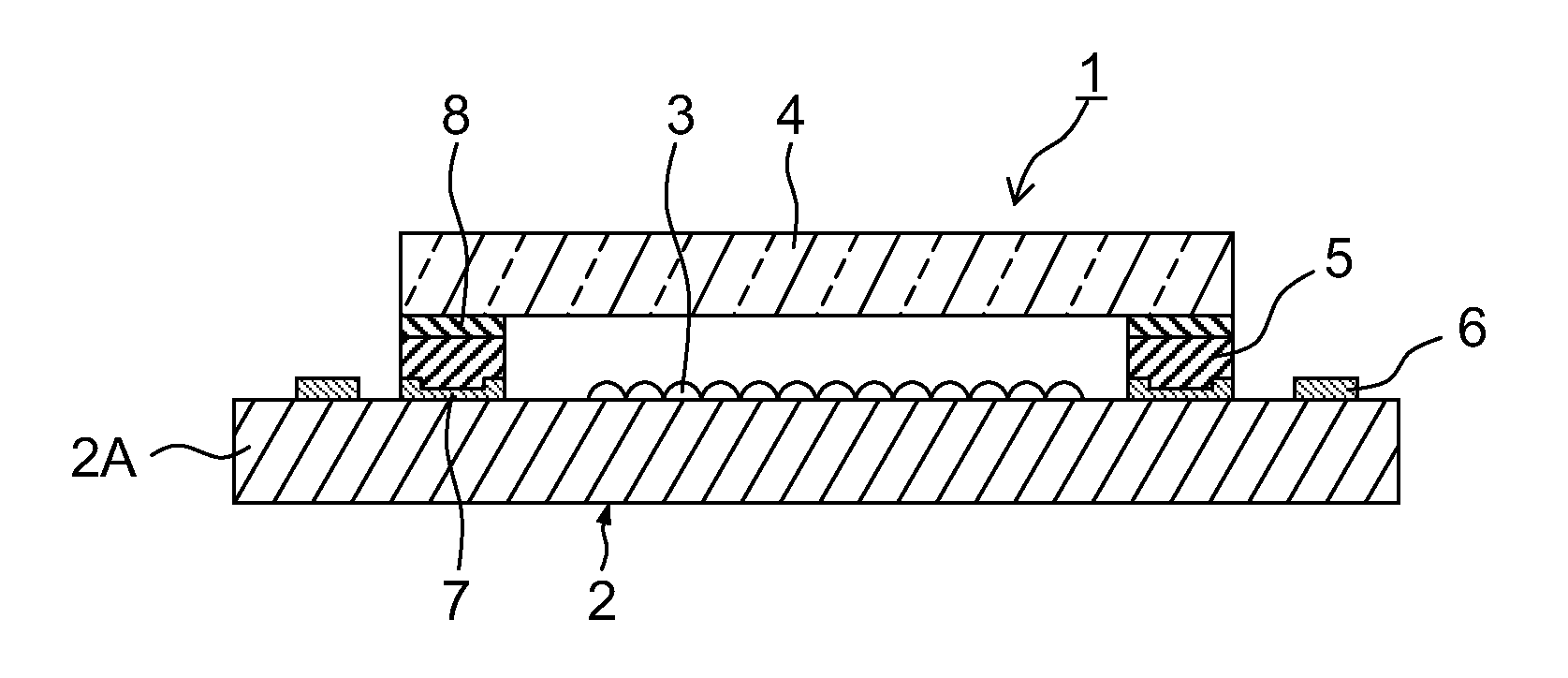
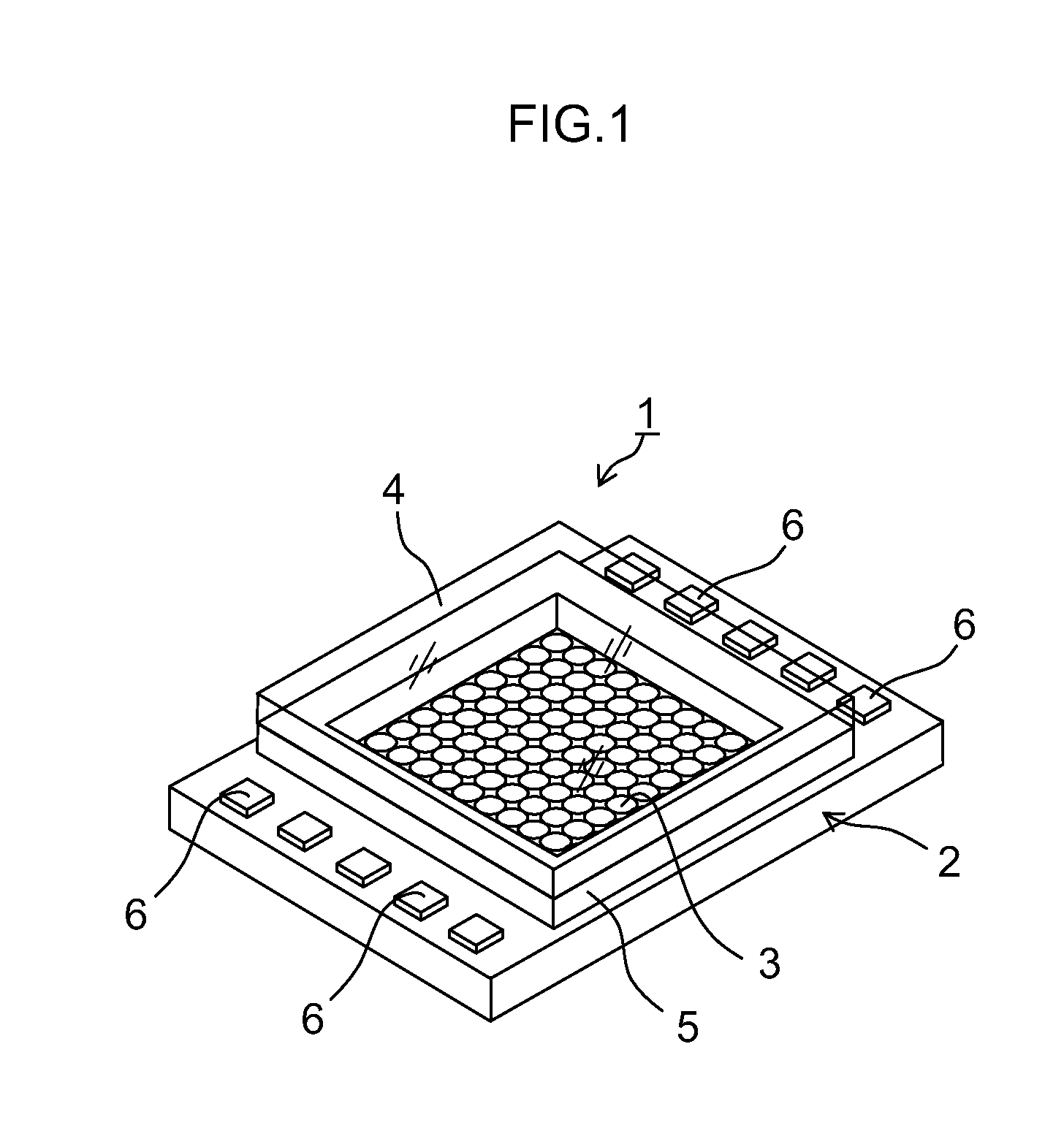
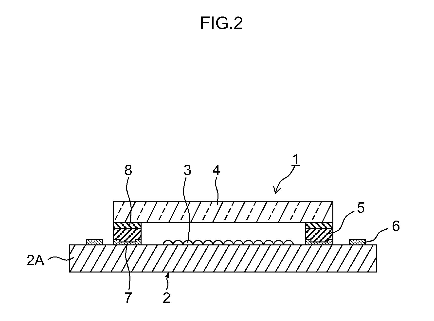
[0023]FIG. 1 and FIG. 2 are a perspective view and a cross sectional view illustrating an appearance configuration of a solid-state image pickup device, respectively. The solid-state image pickup device 1 includes a solid-sta...


PUM

PropertyMeasurementUnit
diameteraaaaaaaaaa
thicknessaaaaaaaaaa
thicknessaaaaaaaaaa

Abstract

Provided is a manufacturing method for a solid-state image pickup device, which enables easily manufacturing a thin-type solid-state image pickup device at a wafer level. A support substrate is bonded to a cover glass substrate. A surface of the cover glass substrate on an opposite side to the support substrate is mechanically polished. A part of the support substrate is removed, and a plurality of frame-shaped spacers are formed on the cover glass substrate. The cover glass substrate is made thinner by wet etching so as to have a predetermined thickness. The cover glass substrate and a silicon wafer on which solid-state image pickup elements are formed are attached to each other via the spacers. The cover glass substrate is divided into individual pieces. The silicon wafer is divided into individual pieces. In this way, the solid-state image pickup device is manufactured.

Description

BACKGROUND OF THE INVENTION[0001]1. Field of the Invention[0002]The presently disclosed subject matter relates to a manufacturing method for a solid-state image pickup device, and more particularly, to a manufacturing method for a thin-type solid-state image pickup device.[0003]2. Description of the Related Art[0004]Against a backdrop of a recent demand for downsizing of devices such as a digital camera and a portable phone, a solid-state image pickup device which is formed of a CCD or a CMOS used in the digital camera and the portable phone is increasingly required to be downsized. Therefore, a shift is being made from a large-sized package in which an entire solid-state image pickup element chip is hermetically sealed to a small-sized package (chip size package: CSP) having a size substantially equal to that of a solid-state image pickup element chip.[0005]There has been proposed a method of manufacturing, collectively on a wafer basis (wafer level), a solid-state image pickup dev...

Claims


Application Information

Patent Timeline
Patent Type & Authority Applications(United States)
IPC IPC(8): H01L31/18
CPCH01L27/14618H01L2924/0002H01L2924/16235H01L2924/00
Inventor WATANABE, MANJIROU
Owner FUJIFILM CORP
Why Eureka
Try Eureka