Multilayered Wiring Board and Method of Manufacturing the Same

a multi-layer wiring and wiring board technology, applied in the direction of printed circuit manufacturing, printed circuit aspects, electrical apparatus construction details, etc., can solve the problems of reducing reliability, difficult to obtain wiring boards, and difficult to obtain insulation properties between wiring lines b>101, so as to increase the adherence area of solder resists, increase the strength of multi-layer wiring boards, and increase the adherence strength of connecting terminals

Inactive Publication Date: 2011-09-01
NGK SPARK PLUG CO LTD
View PDF10 Cites 7 Cited by
  • Summary
  • Abstract
  • Description
  • Claims
  • Application Information

AI Technical Summary

Benefits of technology

[0016]According to the invention described in the first aspect, there is formed a multilayered wiring board as a coreless wiring board which does not have the core board by alternately stacking a plurality of resin insulation layers and a plurality of conductor layers containing the same resin insulation material as a primary or main component. In this multilayered wiring board, a plurality of first main surface side connecting terminals or a plurality of second main surface side connecting terminals are positioned in the openings formed in the outermost resin insulation layer, and the terminal outer surfaces of the connecting terminals are positioned inwardly from the surface of the outermost resin insulation layer. In addition, the solder resist extends into the opening formed in the outermost resin insulation layer and makes contact with the outer circumference portion of each of the terminal outer surfaces so that the outer circumference portion of the terminal outer surface is pressed toward a so-called board thickness direction. Therefore, the connecting terminal is reliably fixed to the outermost resin insulation layer, a gap is not generated between the solder resist and the outer circumference portion of the terminal outer surface, and it is possible to sufficiently increase the adherence strength of the connecting terminal. In addition, since the adherence area of the solder resist for the terminal outer side or the resin insulation layer increases, it is possible to increase the strength of the multilayered wiring board. In addition, since the terminal outer surface of the connecting terminal is not protruded to the solder resist side but buried in the resin insulation layer having a high insulation property, it is possible to sufficiently obtain insulation between the connecting terminals.
[0017]In one implementation, the terminal outer surface is formed with a concavely rounded portion so that the center portion is positioned inwardly from the outer circumference portion. If the connecting terminal is formed in this manner, the adherence area of the solder resist increases. Therefore, it is possible to sufficiently increase adherence with the solder resist. In addition, since the outer circumference portion of the terminal outer side making contact with the solder resist becomes thick, it is possible to improve strength of the terminal.
[0018]In another implementation, the conductor layer, which is located or existing at the interface between the solder resist and the outermost resin insulation layer, includes an interface conductor portion which is embedded in the outermost resin insulation layer. In this manner, the resin insulation layer having a high insulation property is interposed between the conductor layers such as the wiring pattern, and each wiring line can be prepared with a relatively narrow pitch. Therefore, the multilayered wiring board can be highly integrated. Here, as a conductor layer existing at the interface between the solder resist and the outermost resin insulation layer, the multilayered wiring board of the first aspect may include a wiring pattern conductor portion adjacent to the plurality of first main surface side connecting terminals or the plurality of second main surface side connecting terminals. In this case, the outermost resin insulation layer between the plurality of first main surface side connecting terminals or the plurality of second main surface side connecting terminals and the wiring pattern conductor portion may protrude into the solder resist side further than the plurality of first main surface side connecting terminals or the plurality of second main surface side connecting terminals and the wiring pattern conductor portion. If the outermost resin insulation layer protrudes in this manner, since the insulation length between the connecting terminal and the wiring pattern conductor portion increases, it is possible to suppress generation of migration therebetween.
[0019]In yet another implementation, a diameter of openings provided in the solder resist is smaller than a diameter of the openings provided in the outermost resin insulation layer, and the center portion of the terminal outer surface arranged in the opening of the solder resist is formed with a coat metal layer (e.g., a plating layer) made of one or more kinds of metal other than copper. In this case, the coat metal layer does not exist at the interface between the solder resist and the outer circumference portion on the terminal outer surface exposed out of the opening of the solder resist. Here, if, for example, a nickel-gold plating layer is used as the coat metal layer, gold is diffused to the melted solder during the soldering connection. However, according to the present invention, there is no gold plating at the interface between the terminal outer surface and the solder resist. Therefore, it is possible to address a problem that a gap is formed at the interface between the terminal outer surface and the solder resist due to diffusion of gold to the solder. As a result, it is possible to allow the terminal outer surface and the solder resist to reliably abut on each other, and sufficiently obtain adherence strength of the connecting terminal even after forming the solder on the connecting terminal.
[0020]In still yet another implementation, the solder resist is arranged on the second main surface side of the stack structure, and a plurality of motherboard connecting terminals to be connected to a motherboard are the plurality of second main surface side connecting terminals. In this case, the motherboard connecting terminals require a relatively large area and high adherence strength. However, since the solder resist is inserted into the opening as described above, the outer circumference portion of the terminal outer surfaces are pressed toward a so-called board thickness direction. Therefore, it is possible to obtain sufficient adherence strength in the motherboard connecting terminals and improve reliability of the multilayered wiring board. In addition, the solder resist may be provided on the main surface side where the motherboard is connected or on the opposite side to the main surface, for example, in the main surface side where the IC chip is installed.
[0021]In still yet another implementation, the via conductors are tapered such that the diameters thereof are widened from the second main surface side to the first main surface side. Inversely, all of the via conductors formed in a plurality of resin insulation layers may be tapered such that the diameters thereof are widened from the first main surface side to the second main surface side. In this manner, it is possible to reliably manufacture the coreless wiring board without the core board.

Problems solved by technology

Therefore, in this case, it is difficult to obtain wiring boards 100A and 100B having a high reliability.
Therefore, when the wiring line 101 is provided to be protruded in the solder resist 104 side as in the wiring lines 100A and 100B, it may be difficult to obtain an insulation property between the wiring lines 101 due to a high density tendency of the wiring lines 101.
In addition, this also causes reduced reliability.

Method used


Image

  • Multilayered Wiring Board and Method of Manufacturing the Same
  • Multilayered Wiring Board and Method of Manufacturing the Same
  • Multilayered Wiring Board and Method of Manufacturing the Same

Examples


Embodiment Construction

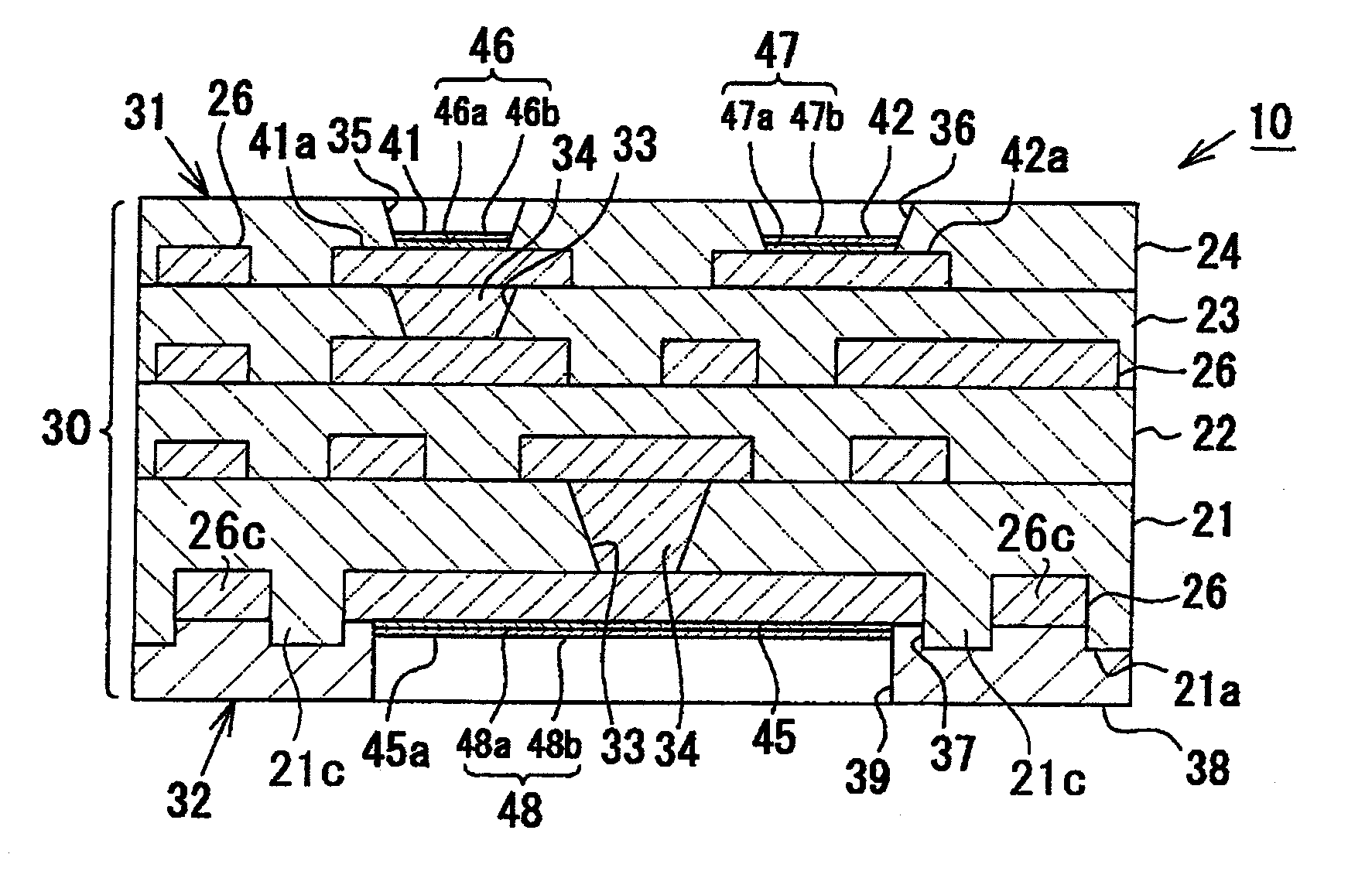
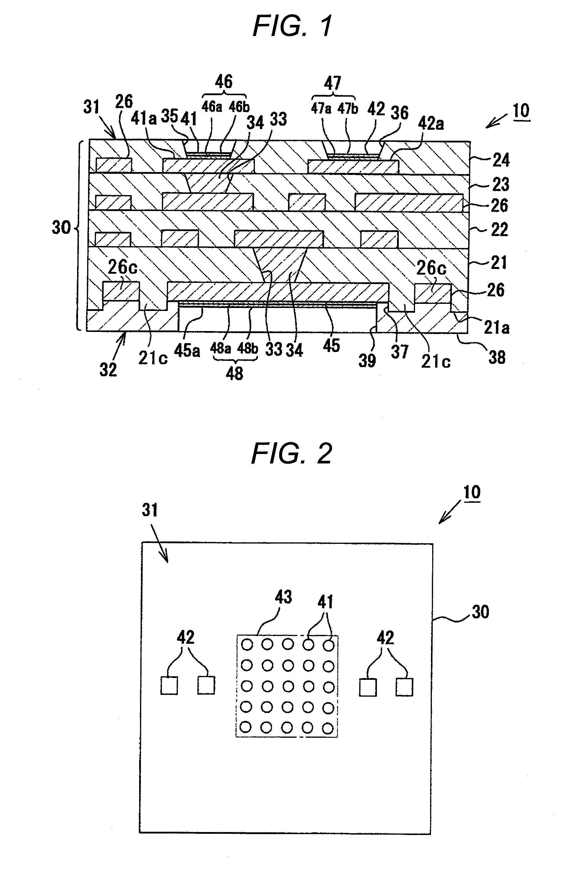
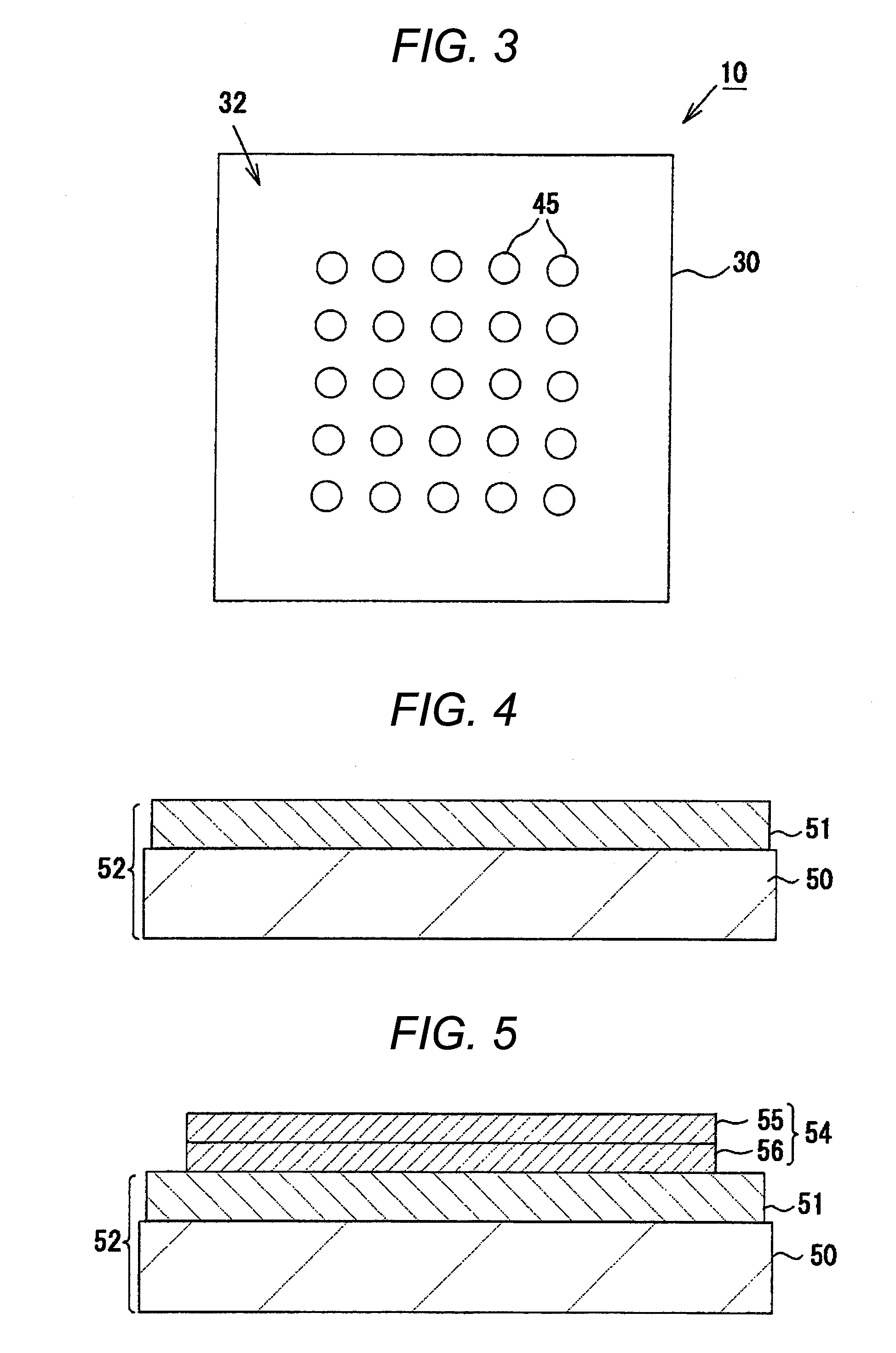
[0046]Hereinafter, a multilayered wiring board according to an embodiment of the present invention will be described in detail with reference to the accompanying drawings. FIG. 1 is an enlarged cross-sectional view illustrating a schematic configuration of the multilayered wiring board according to the present embodiment. In addition, FIG. 2 is a plan view illustrating the multilayered wiring board viewed from the upper surface side, and FIG. 3 is a plan view illustrating the multilayered wiring board viewed from the bottom surface side.

[0047]Referring to FIG. 1, the multilayered wiring board 10 is a coreless wiring board which does not have the core board but has a wiring stack portion30 (stack structure) multilayered by alternately stacking four resin insulation layers 21, 22, 23 and 24 including a same resin insulation material as a main component and a conductor layer 26 made of copper. Each resin insulation layer 21 to 24 is formed using a build-up material including a resin in...


PUM

PropertyMeasurementUnit
diametersaaaaaaaaaa
circumferenceaaaaaaaaaa
diameteraaaaaaaaaa

Abstract

A multilayered wiring board having a stack structure multilayered by alternately stacking a plurality of conductor layers and a plurality of resin insulation layers, wherein a solder resist is provided on at least one of a first main surface side and a second main surface side of the stack structure, a plurality of openings are formed in an outermost resin insulation layer that contacts with the solder resist, a plurality of the first main surface side connecting terminals or a plurality of the second main surface side connecting terminals being made of a copper layer as a main component and positioned in a plurality of the openings, terminal outer surfaces being positioned inwardly from an outer surface of the outermost resin insulation layer, and the solder resist extends into the plurality of openings and makes contact with an outer circumference portion of each of the terminal outer surfaces.

Description

CROSS REFERENCE TO RELATED APPLICATION[0001]The present application claims priority from Japanese Patent Application No. 2010-041470, which was filed on Feb. 26, 2010, the disclosure of which is herein incorporated by reference in its entirety.BACKGROUND OF THE INVENTION[0002]1. Field of the Invention[0003]The present invention relates to a multilayered wiring board having a stack structure multilayered by alternately stacking a plurality of resin insulation layers including a same resin insulation material as a main component and a plurality of conductor layers and without a so-called core board by sequentially forming build-up layers on both sides of the structure, and a method of manufacturing the same.[0004]2. Description of Related Art[0005]A semiconductor integrated circuit device (IC chip) used as a microprocessor of a computer or the like has recently become more and more rapid and multifunctional. Accordingly, the number of terminals tends to increase, and a pitch between t...

Claims


Application Information

Patent Timeline
Patent Type & Authority Applications(United States)
IPC IPC(8): H05K1/11H01R9/00
CPCH05K1/112H05K3/205H05K3/4682Y10T29/49147H05K2201/09472H05K2201/099H05K2201/094H05K1/11H05K3/46
Inventor MAEDA, SHINNOSUKEHIRANO, SATOSHI
Owner NGK SPARK PLUG CO LTD
Why Eureka
Try Eureka