
Semiconductor light emitting device having multi-cell array, light emitting module, and illumination apparatus

a light-emitting device and semiconductor technology, applied in the direction of semiconductor devices, basic electric elements, electrical equipment, etc., can solve the problems of high-power leds using high-rated currents that have low light efficiency, accelerate light efficiency degradation, and reduce the efficiency of light-emitting cells. , to achieve the effect of improving the light efficiency of the defective light-emitting cell, improving the current density per unit area, and improving the light efficiency

Active Publication Date: 2011-09-01
SAMSUNG ELECTRONICS CO LTD
View PDF8 Cites 50 Cited by
  • Summary
  • Abstract
  • Description
  • Claims
  • Application Information

AI Technical Summary

Benefits of technology

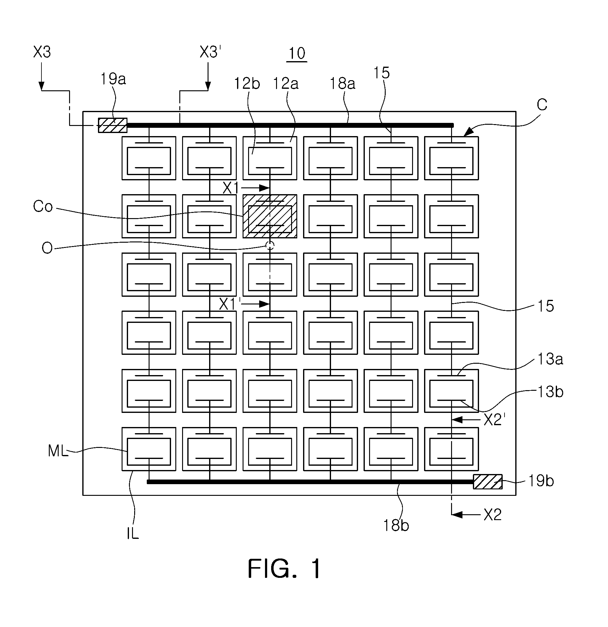
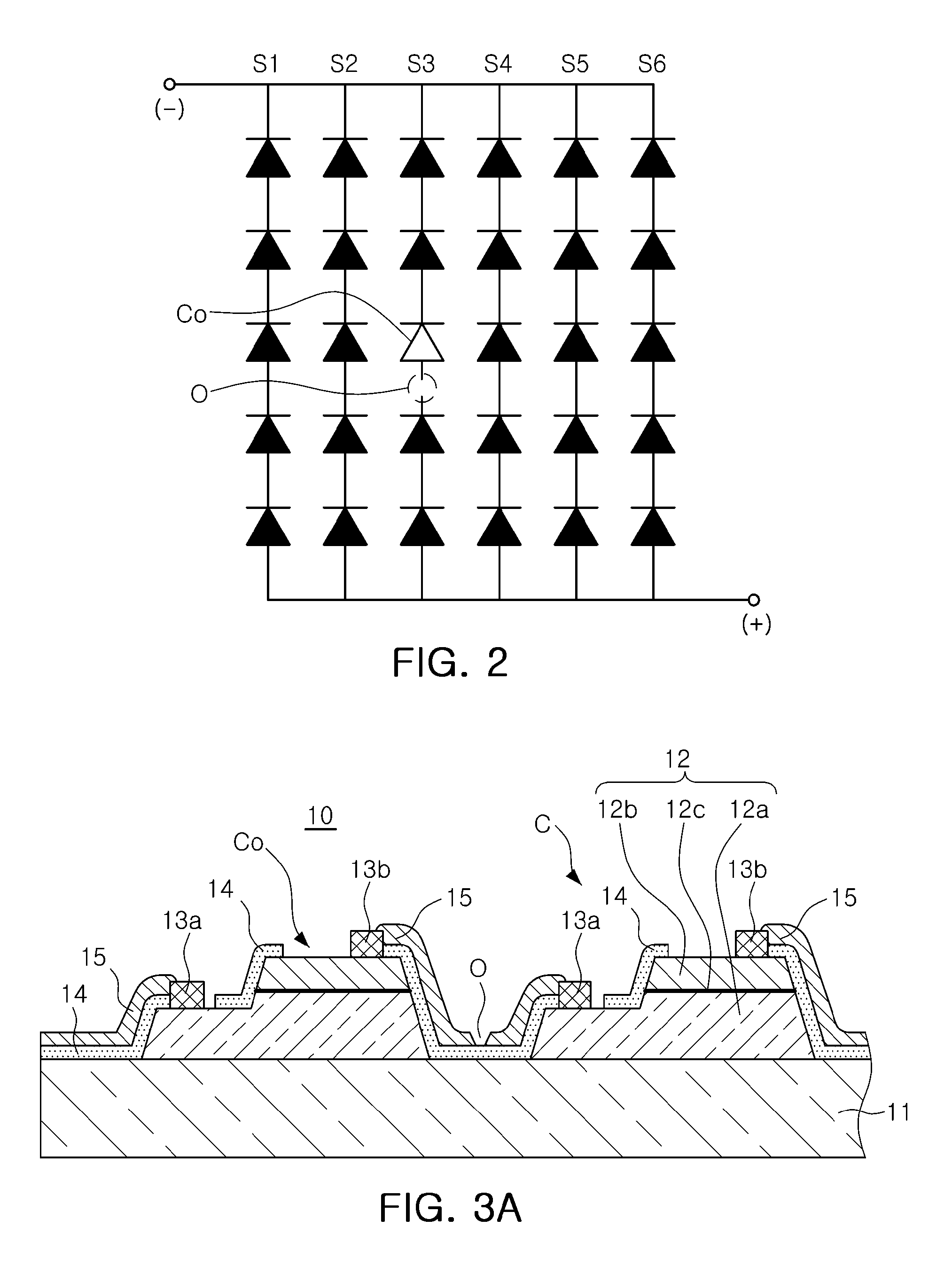
The present invention provides a semiconductor light emitting device that improves current density per unit area to improve light efficiency and process defective light emitting cells effectively. The device includes a substrate, light emitting cells, and connection parts to connect the cells in a parallel or series-parallel configuration. The light emitting cells have improved connection structures to facilitate easy implementation of various interconnection structures. The device also includes an insulation layer to prevent undesired connections between the connection parts and light emitting cells. The light emitting cells may be arrayed in columns with the same number of cells in each column. The connection parts may include first and second connection parts connected to the first-conductivity-type semiconductor layer and the second-conductivity-type semiconductor layer of the light emitting cells. The device has improved processing efficiency and can be used in various applications such as lighting apparatus and illumination.

Problems solved by technology

However, a high-power LED using a high-rated current may have low light efficiency due to a high current density, when compared to a low-power LED using a low-rated current.
Specifically, if a rated current is increased to obtain high luminous flux in an LED chip of the same area in order to obtain high power, the light efficiency may be degraded due to an increase in the current density.
Also, the light efficiency degradation is accelerated due to heat generated by the device.

Method used


Image

  • Semiconductor light emitting device having multi-cell array, light emitting module, and illumination apparatus
  • Semiconductor light emitting device having multi-cell array, light emitting module, and illumination apparatus
  • Semiconductor light emitting device having multi-cell array, light emitting module, and illumination apparatus

Examples


first embodiment

[0107]FIGS. 7 through 11 illustrate various embodiments using an intermediate connection part, as a scheme for satisfying the above requirements in the series-parallel connection structure like the

[0108]Referring to FIG. 7, a multi-cell array semiconductor light emitting device 70 according to this embodiment includes a substrate 71, and a plurality of light emitting cells C arrayed in a 6×4 pattern on the top surface of the substrate 71. Like the aforesaid embodiment, the light emitting cells C may be obtained by dividing a semiconductor multilayer structure having a first-conductivity-type semiconductor layer, an active layer, and a second-conductivity-type semiconductor layer that are sequentially formed on the top surface of the substrate 71.

[0109]In this embodiment, an isolation process is performed to entirely remove the semiconductor multilayer structure (a complete isolation process) to expose the surface of the substrate 71. Also, the first-conductivity-type semiconductor l...

third embodiment

[0140]FIG. 13 is a top plan view illustrating a multi-cell array semiconductor light emitting device according to the present invention. FIG. 14 is an equivalent circuit diagram of a multi-cell array implemented in the multi-cell array semiconductor light emitting device illustrated in FIG. 13.

[0141]Referring to FIG. 13, a multi-cell array semiconductor light emitting device 130 according to this embodiment includes a substrate 131, and a plurality of light emitting cells C arrayed in a 6×4 pattern on the top surface of the substrate 131.

[0142]Like the aforesaid embodiment, the light emitting cells C may be obtained by dividing a semiconductor multilayer structure having a first-conductivity-type semiconductor layer, an active layer, and a second-conductivity-type semiconductor layer that are sequentially formed on the top surface of the substrate 131.

[0143]In this embodiment, a complete isolation process is performed to isolate the semiconductor multilayer structure by light emitti...


PUM


Abstract

A semiconductor light emitting device includes a substrate; a plurality of light emitting cells disposed on the top surface of the substrate, the light emitting cells each having an active layer; a plurality of connection parts formed on the substrate with the light emitting cells formed thereon to connect the light emitting cells in a parallel or series-parallel configuration; and an insulation layer formed on the surface of the light emitting cell to prevent an undesired connection between the connection parts and the light emitting cell. The light emitting cells comprise at least one defective light emitting cell, and at least one of the connection parts related to the defective light emitting cell is disconnected.

Description

CROSS-REFERENCE TO RELATED APPLICATIONS[0001]This application claims the priority of Korean Patent Application No. 10-2010-0018277 filed on Feb. 27, 2010, in the Korean Intellectual Property Office, the disclosure of which is incorporated herein by reference.BACKGROUND OF THE INVENTION[0002]1. Field of the Invention[0003]The present invention relates to a semiconductor light emitting device, and more particularly, to a semiconductor light emitting device having an array of light emitting cells, a light emitting module including the semiconductor light emitting device, and an illumination apparatus including the light emitting module.[0004]2. Description of the Related Art[0005]In general, semiconductor light emitting diodes (LEDs) are advantageous for light sources in terms of power, efficiency and reliability. Therefore, semiconductor LEDs are being actively developed as high-power, high-efficiency light sources for various illumination apparatuses as well as for backlight units of...

Claims


Application Information

Patent Timeline
Patent Type & Authority Applications(United States)
IPC IPC(8): H01L33/08
CPCH01L27/153H01L27/156H01L33/30H01L33/62H01L2224/48091H01L2924/12041H01L24/24H01L2924/00014H01L2924/00H01L2924/12042H01L33/48
Inventor LEE, SU YEOLKIM, YONG TAELEE, JIN BOCKKIM, GI BUM
Owner SAMSUNG ELECTRONICS CO LTD
Learn More