P-channel power mosfet

a power mosfet and p-channel technology, applied in the field of p-channel power mosfet, can solve the problems of poor reliability and disadvantages of the n-channel power mosfet structure, and achieve the effect of reducing the degree of deterioration

Inactive Publication Date: 2011-09-08
RENESAS ELECTRONICS CORP
View PDF17 Cites 30 Cited by
  • Summary
  • Abstract
  • Description
  • Claims
  • Application Information

AI Technical Summary

Benefits of technology

[0014]To sum up, the following advantageous effect is provided according to the representative aspects of the present invention:
[0015]A p-channel power MOSFET configured to have an n-type polysilicon linear field plate electrode and an n-type p

Problems solved by technology

In characteristic test measurements of these double-gate-in-trench p-channel power MOSFETs each having a p+ polysilicon gate electrode and a p+ field plate electrode in a trench, it has been found that there are disadvantageous problems in comparison with the n-channel power MOS

Method used


Image

  • P-channel power mosfet
  • P-channel power mosfet
  • P-channel power mosfet

Examples


Embodiment Construction

Overviews of the Preferred Embodiments

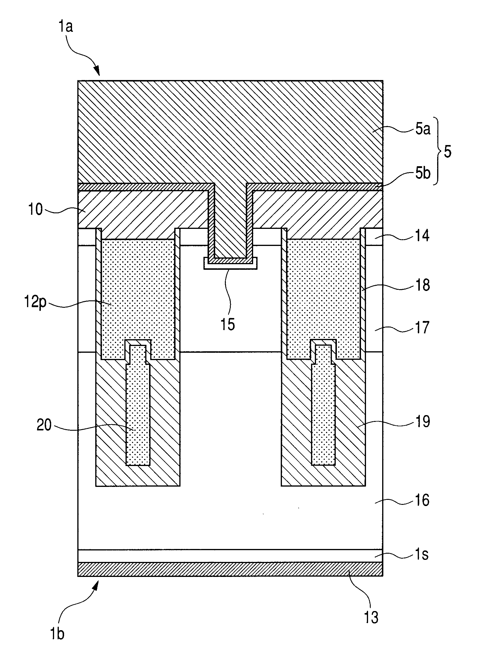
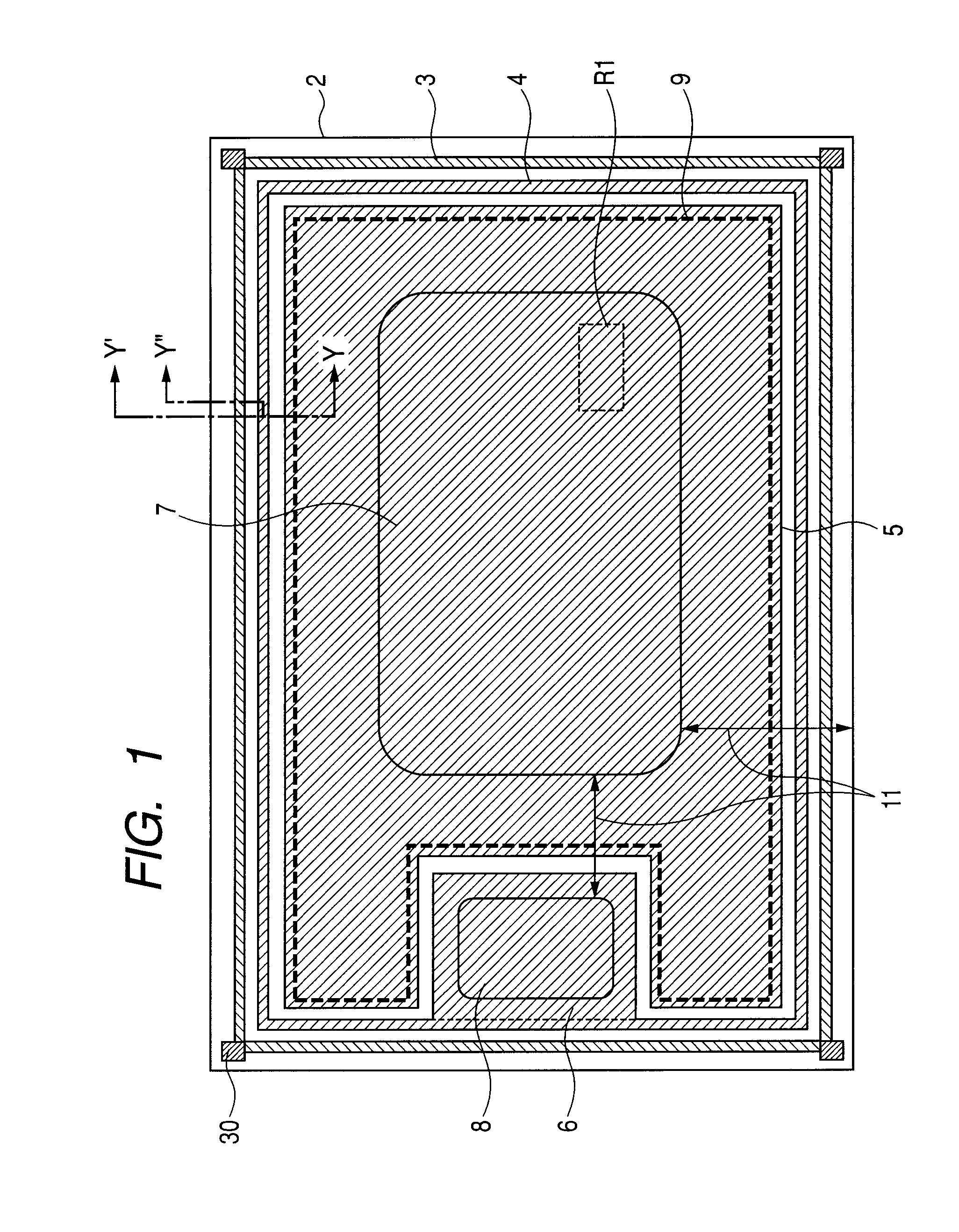
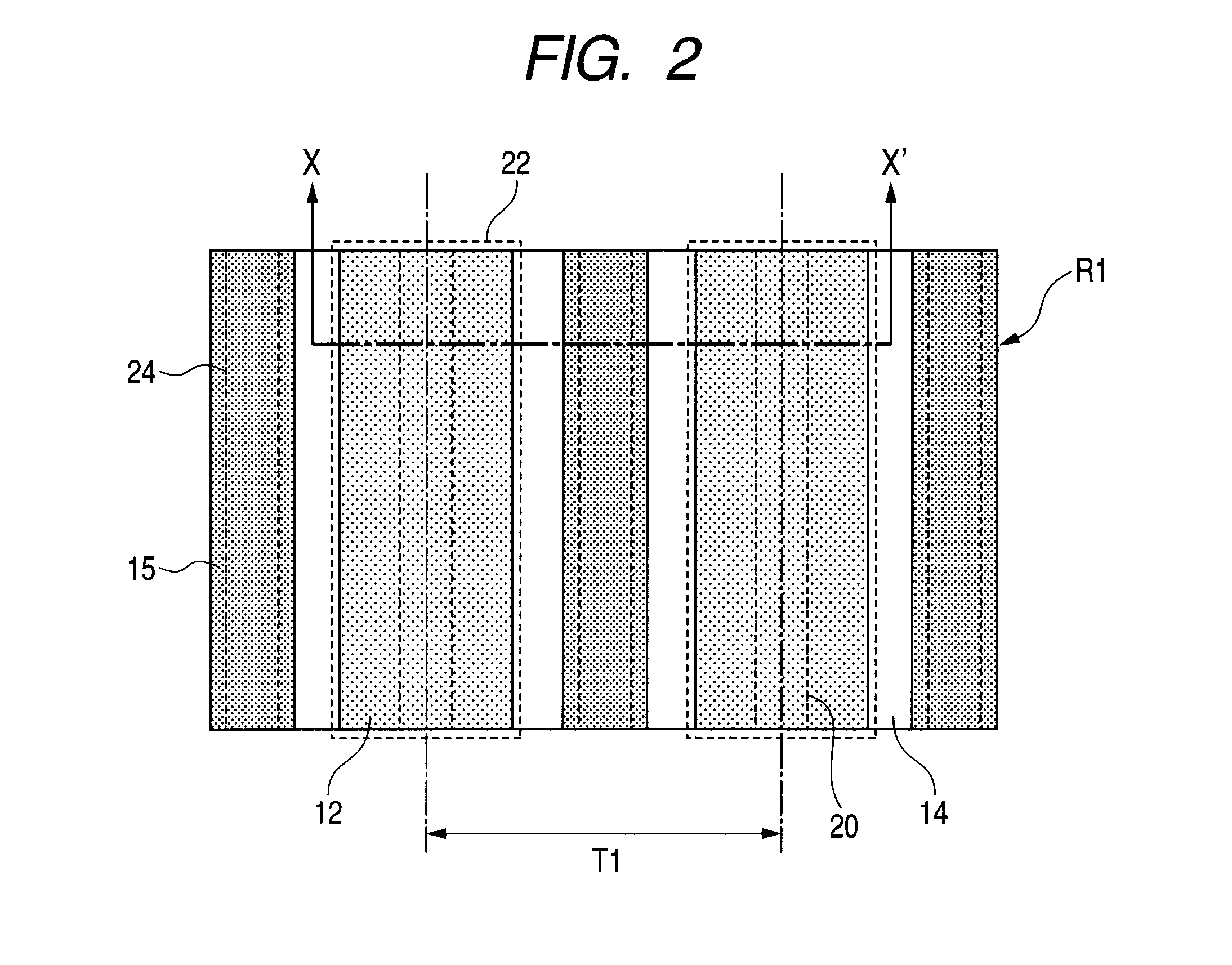
[0046]First, the present invention will be described below regarding the overviews of representative preferred embodiments thereof.[0047]1. In accordance with a representative preferred embodiment of the present invention, there is provided a p-channel power MOSFET comprising: (a) a silicon-based semiconductor substrate having first and second principal surface sides; and (b) a multiplicity of linear trenches disposed in the first principal surface side. Each of the linear trenches includes: (b1) an n-type polysilicon linear field plate electrode; and (b2) an n-type polysilicon linear gate electrode disposed over and along the n-type polysilicon linear field plate electrode.[0048]2. In the p-channel power MOSFET mentioned in item 1, the second principal surface side of the silicon-based semiconductor substrate is provided with a p-type silicon single-crystal substrate region.[0049]3. In the p-channel power MOSFET mentioned in item 2, the first p...


PUM


Abstract

In characteristic test measurements of double-gate-in-trench p-channel power MOSFETs each having a p+ polysilicon gate electrode and a p+ field plate electrode in a trench, which were fabricated according to common design techniques, it has been found that, under conditions where a negative gate bias is applied continuously at high temperature with respect to the substrate, an absolute value of threshold voltage tends to increase steeply after the lapse of a certain period of stress application time. To solve this problem, the present invention provides a p-channel power MOSFET having an n-type polysilicon linear field plate electrode and an n-type polysilicon linear gate electrode in each trench part thereof.

Description

CROSS-REFERENCE TO RELATED APPLICATIONS[0001]The disclosure of Japanese Patent Application No. 2010-46452 filed on Mar. 3, 2010 including the specification, drawings and abstract is incorporated herein by reference in its entirety.BACKGROUND OF THE INVENTION[0002]The present invention relates to semiconductor devices, and more particularly to a semiconductor integrated circuit device technique that is effectively applicable to a MOSFET device.[0003]In Japanese Unexamined Patent Publication No. 2006-202931 (Patent Document 1) or U.S. Patent Application Publication No. 2006-157779 (Patent Document 2) corresponding thereto, there is disclosed an n-channel MOSFET wherein a field plate electrode is disposed under an ordinary trench gate electrode.Related Art References—Patent Documents:[0004]Patent Document 1:[0005]Japanese Unexamined Patent Publication No. 2006-202931[0006]Patent Document 2:[0007]U.S. Patent Application Publication No. 2006-157779SUMMARY OF THE INVENTION[0008]In the eng...

Claims


Application Information

Patent Timeline
IPC IPC(8): H01L29/78
CPCH01L29/78H01L29/407H01L29/7813H01L29/66734H01L29/42376H01L29/7811H01L29/66727H01L29/41H01L29/0619H01L29/4983
Inventor MATSUURA, HITOSHINAKAZAWA, YOSHITO
Owner RENESAS ELECTRONICS CORP
Why Eureka
Try Eureka