OLED circuit compensation method

A compensation method and circuit technology, applied in instruments, static indicators, etc., can solve problems such as poor pixel luminous effect, and achieve the effects of solving poor display effect, increasing yield, and reducing deterioration.

Inactive Publication Date: 2020-02-21
FUJIAN HUAJIACAI CO LTD
View PDF17 Cites 4 Cited by
  • Summary
  • Abstract
  • Description
  • Claims
  • Application Information

AI Technical Summary

Problems solved by technology

[0007] For this reason, it is necessary to provide a new pixel compensation method to solve the problem of poor lighting effect of pixels in the prior art

Method used


Image

  • OLED circuit compensation method
  • OLED circuit compensation method
  • OLED circuit compensation method

Examples


Embodiment Construction

[0021] In order to explain in detail the technical content, structural features, achieved goals and effects of the technical solution, the following will be described in detail in conjunction with specific embodiments and accompanying drawings.

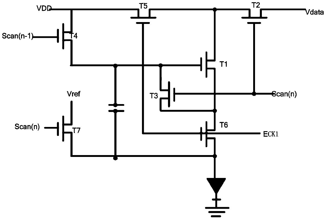
[0022] see figure 1 , a total of seven TFT transistors and a capacitor, that is, 7T1C design, the transistor is an N-type structure. We can see from the figure that an OLED circuit compensation method is characterized in that it is suitable for OLED circuits, and the OLED circuit includes thin film transistors T1, T2, T3, T4, T5, T6, T7, capacitor C1, power supply voltage VDD is connected to the source of T5 and the source of T4, the gate of T5 is connected to the gate of T6 and connected to the clock signal line, the drain of T5 is connected to the sources of T1 and T2; the T4 The gate of T3 is connected with the scan signal of the previous stage, and the drain is connected with the source of T3 and the gate of T1; the gate of T3 is...


PUM


Abstract

The invention discloses an OLED circuit compensation method. The circuit compensation method comprises a reset stage, a threshold voltage extraction stage, a maintenance stage, a light-emitting stageand a rest stage, wherein the clock signal line is a square wave pulse, the clock signal line comprises a first low level, a first high level and a second low level square wave signal which are continuous, the first low level comprises a reset stage, a threshold voltage extraction stage and a maintenance stage, the first high level is a light-emitting stage, and the second low level is a rest stage; wherein the previous-stage scanning signal is at a high level in a reset stage and at a low level in other time, and the current-stage scanning signal is at a high level in a threshold voltage extraction stage and at a low level in other time periods. According to the scheme, an Em GIP drive circuit is not needed, so that three advantages are brought: 1, the OLED can have a recovery rest stage,and the deterioration degree of the OLED is reduced; 2, a complex Em drive circuit does not need to be designed, and the yield is increased; 3, an Em circuit is not needed, so that narrow-frame design is facilitated;

Description

technical field [0001] The invention relates to a pixel circuit display optimization technology, in particular to a novel OLED pixel driving compensation method. Background technique [0002] Organic light emitting diodes (Organic Light Emitting Diode, OLED) can be divided into passive matrix driving (Passive Matrix OLED, PMOLED) and active matrix driving (Active Matrix OLED, AMOLED) according to the driving method. Among them, the PMOLED does not emit light when data is not written, but only emits light during data writing. This driving method is simple in structure, low in cost, and easy to design, and is mainly suitable for small and medium-sized displays. [0003] Finally, AM stands for Active Matrix, which is relative to Passive Matrix and refers to the driving method of each OLED pixel. In Passive Matrix, the control of each pixel is realized through a complex electrode network, so as to realize the charge and discharge of a certain pixel. Generally speaking, the con...

Claims


Application Information

Patent Timeline
Patent Type & Authority Applications(China)
IPC IPC(8): G09G3/3225
CPCG09G3/3225
Inventor 曹尚操朱书纬
Owner FUJIAN HUAJIACAI CO LTD
Why Eureka
Try Eureka