Method for manufacturing semiconductor device, and semiconductor device

a manufacturing method and semiconductor technology, applied in semiconductor devices, capacitors, electrical devices, etc., can solve the problems of difficult to enter hydrogen into the ferroelectric capacitor, difficult to reach the ferroelectric film etc., and achieve the effect of diminishing the degree of deterioration of the ferroelectric capacitor

Active Publication Date: 2007-05-29
SEIKO EPSON CORP
View PDF3 Cites 5 Cited by
  • Summary
  • Abstract
  • Description
  • Claims
  • Application Information

AI Technical Summary

Benefits of technology

[0027]According to the method for manufacturing a semiconductor device, the ferroelectric capacitor is covered by the first hydrogen barrier film and the third hydrogen barrier film without any gap. Accordingly, even when hydrogen degasses from the dielectric film located below the ferroelectric capacitor, the hydrogen is difficult to enter the ferroelectric capacitor. Accordingly, the electrical characteristics of the ferroelectric capacitor are difficult to deteriorate.
[0029]In contrast, according to the method for manufacturing a semiconductor device described above, because the intermediate layer composed of a film having a lower internal stress compared to the first hydrogen barrier film is formed on the first hydrogen barrier film, the first hydrogen barrier film is protected by the intermediate layer. Accordingly, the hydrogen barrier capability of the first hydrogen barrier film is difficult to deteriorate.
[0030]Although hydrogen may be occluded in the intermediate layer, the intermediate layer is removed while leaving a portion thereof located below the ferroelectric capacitor and its marginal area before the third hydrogen barrier film is formed in accordance with the method for manufacturing a semiconductor device described above. For this reason, hydrogen becomes more difficult to enter the ferroelectric capacitor. It is noted that, in the removal step, hydrogen may be generated in the atmosphere. However, because the upper surface and side surfaces of the ferroelectric capacitor are covered by the second hydrogen barrier film before the removal step, the degree of deterioration of the ferroelectric capacitor becomes diminished.
[0041]According to the method for manufacturing a semiconductor device, the ferroelectric capacitor is covered by the first hydrogen barrier film and the third hydrogen barrier film without any gap. Accordingly, even when hydrogen degasses from the dielectric film located below the ferroelectric capacitor, the hydrogen is difficult to enter the ferroelectric capacitor. Accordingly, the electrical characteristics of the ferroelectric capacitor are difficult to deteriorate.
[0042]In each of the methods for manufacturing a semiconductor device described above, the present invention is particularly effective when the dielectric film is formed by a CVD method using a starting material including hydrogen as a starting material.

Problems solved by technology

For this reason, even when hydrogen or the like is generated in a step after the ferroelectric capacitor has been formed, the hydrogen is difficult to reach the ferroelectric film of the ferroelectric capacitor.
In this case, there is a possibility that the degassed hydrogen or the like may reach the ferroelectric capacitor, and may deteriorate the ferroelectric capacitor.
Accordingly, even when hydrogen degasses from the dielectric film located below the ferroelectric capacitor, the hydrogen is difficult to enter the ferroelectric capacitor.
Accordingly, the electrical characteristics of the ferroelectric capacitor are difficult to deteriorate.
It is noted that, when the first hydrogen barrier film has a large internal stress, there is a possibility that the internal stress may affect the electrical characteristics of the ferroelectric capacitor.
In this embedding step, there is a possibility that the first hydrogen barrier film may be damaged, and its hydrogen barrier capability may be lowered.
Accordingly, the hydrogen barrier capability of the first hydrogen barrier film is difficult to deteriorate.
For this reason, hydrogen becomes more difficult to enter the ferroelectric capacitor.
However, because the upper surface and side surfaces of the ferroelectric capacitor are covered by the second hydrogen barrier film before the removal step, the degree of deterioration of the ferroelectric capacitor becomes diminished.
Accordingly, even when hydrogen degasses from the dielectric film located below the ferroelectric capacitor, the hydrogen is difficult to enter the ferroelectric capacitor.
Accordingly, the electrical characteristics of the ferroelectric capacitor are difficult to deteriorate.
In the heating step, even when hydrogen or the like degasses from the interlayer dielectric film located below the ferroelectric capacitor, the hydrogen or the like is difficult to enter the ferroelectric capacitor.
Accordingly, the electrical characteristics of the ferroelectric capacitor become difficult to deteriorate.

Method used


Image

  • Method for manufacturing semiconductor device, and semiconductor device
  • Method for manufacturing semiconductor device, and semiconductor device
  • Method for manufacturing semiconductor device, and semiconductor device

Examples


Embodiment Construction

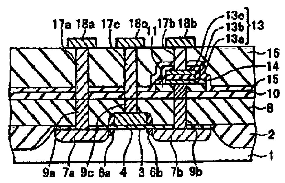
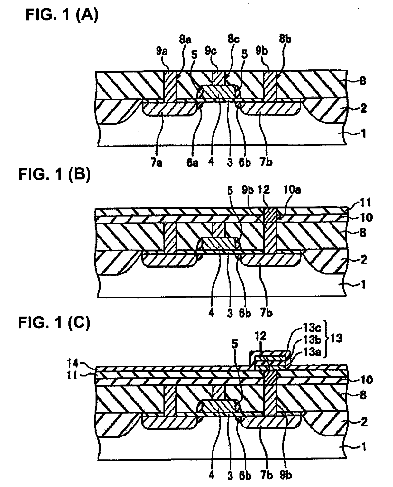
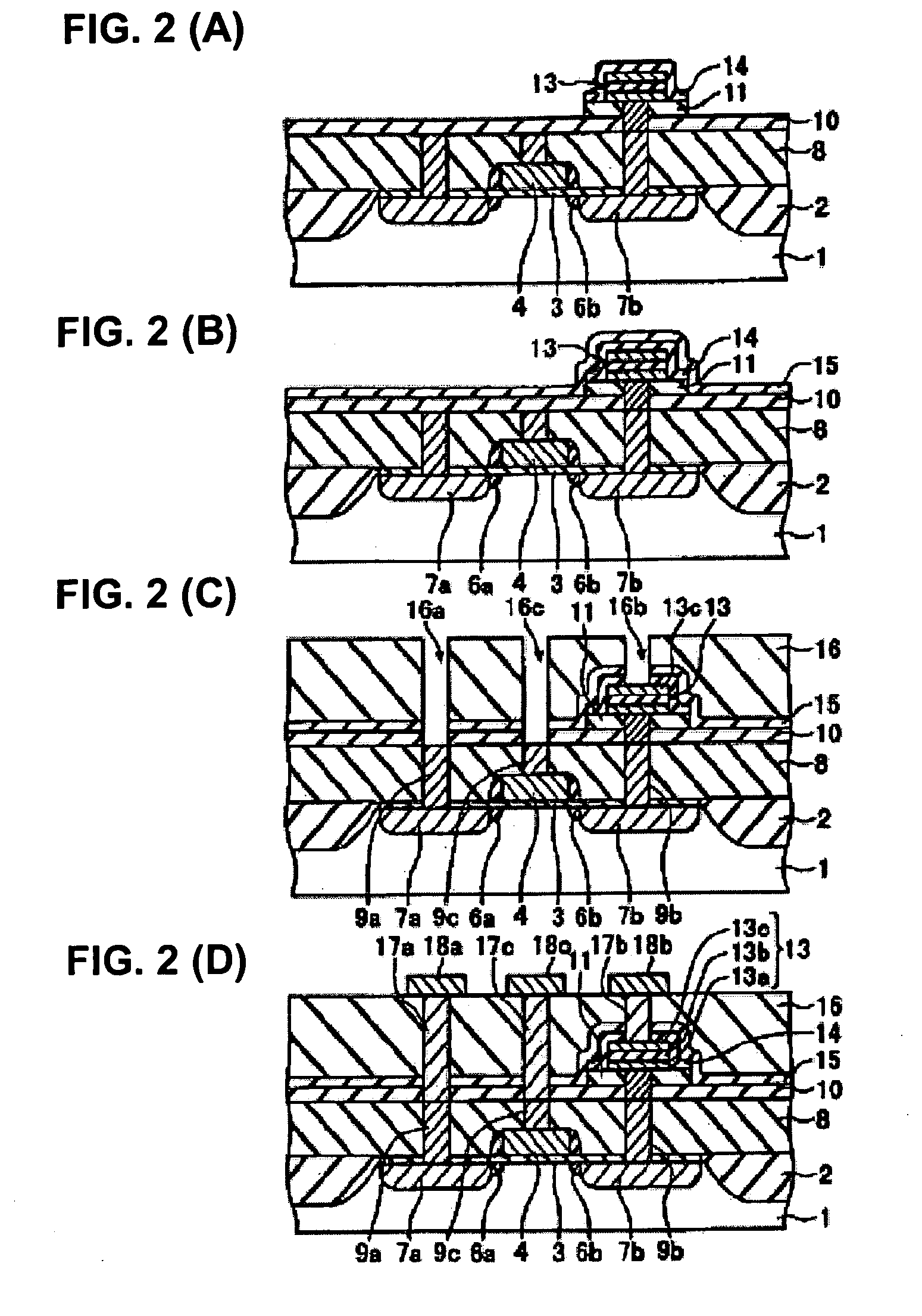
[0089]Embodiments of the present invention are described below with reference to the accompanying drawings. FIG. 1 and FIG. 2 are cross-sectional views for describing a method for manufacturing a semiconductor device in accordance with a first embodiment. The present embodiment pertains to a method for forming a stacked type ferroelectric memory.

[0090]First, as shown in FIG. 1 (A), an element isolation film 2 is formed in a silicon substrate 1 by, for example, a LOCOS method. The element isolation film 2 is open above an element region. Next, the silicon substrate 1 is thermally oxidized. By this, a gate oxide film 3 is formed on the silicon substrate 1 located at the element region. Next, a polysilicon film is formed over the entire surface including on the gate oxide film 3, and the polysilicon film is patterned. By this, a gate electrode 4 is formed on the gate oxide film 3. Next, by using the gate electrode 4 and the element isolation film 2 as a mask, impurity ions are injected...


PUM

PropertyMeasurementUnit
thicknessaaaaaaaaaa
thicknessaaaaaaaaaa
thicknessaaaaaaaaaa

Abstract

A first hydrogen barrier film and an intermediate layer are formed on an interlayer dielectric film. A ferroelectric capacitor is formed on the intermediate layer, and a second hydrogen barrier film is formed over the entire surface including on the upper surface and side surfaces of the ferroelectric capacitor and on the intermediate layer. Then, the second hydrogen barrier film and the intermediate layer are removed while leaving at least portions on the upper surface and side surfaces of the ferroelectric capacitor. Then, a third hydrogen barrier film is formed on the second hydrogen barrier film, on side surfaces of the second hydrogen barrier film and the intermediate layer, and on the first hydrogen barrier film.

Description

RELATED APPLICATIONS[0001]This application claims priority to Japanese Patent Application No. 2004-181353 filed Jun. 18, 2004 which is hereby expressly incorporated by reference herein in its entirety.BACKGROUND[0002]1. Technical Field[0003]The present invention relates to methods for manufacturing semiconductor devices having ferroelectric capacitors, and semiconductor devices. In particular, the present invention relates to a method for manufacturing a semiconductor device in which a ferroelectric capacitor is protected from hydrogen included in a lower layer thereof, such that electrical characteristics of the ferroelectric capacitor are difficult to deteriorate, and also relates to such a semiconductor device.[0004]2. Related Art[0005]FIGS. 5(A) and (B) are cross-sectional views for describing a conventional method for manufacturing a semiconductor device having a ferroelectric capacitor. First, as shown in FIG. 5 (A), an element isolation film 102 is formed in a silicon substra...

Claims


Application Information

Patent Timeline
Patent Type & Authority Patents(United States)
IPC IPC(8): H01L21/00H01L21/20H01L21/02H01L21/8246H01L27/105H01L27/115H01L29/76
CPCH01L27/11502H01L27/11507H01L28/57H10B53/30H10B53/00H01L27/04H10B12/00
Inventor TAKANO, KATSUO
Owner SEIKO EPSON CORP
Why Eureka
Try Eureka