Semi-polar iii-nitride optoelectronic devices on m-plane substrates with miscuts less than +/-15 degrees in the c-direction

a technology of iii-nitride and mplane, which is applied in the direction of semiconductor devices, lasers, semiconductor lasers, etc., can solve the problems of blue-shift in emission wavelength, qcse becomes more significant for long wavelength optoelectronic devices, and the m-plane lds has so far been limited to 500 nm lasing emission, etc., to achieve low qcse induced injection-current dependent blu

Active Publication Date: 2011-09-08
RGT UNIV OF CALIFORNIA
View PDF25 Cites 258 Cited by
  • Summary
  • Abstract
  • Description
  • Claims
  • Application Information

AI Technical Summary

Benefits of technology

[0018]Such optoelectronic devices, on an m-plane with x degrees of miscut towards the c-direction (where −15<x<−1 and 1<x<15 degrees), provide lower QCSE induced injection-current dependent blue-shift, increased oscillator strength leading to higher material gain, etc., compared to miscuts larger or equal to +/−15 degrees towards the c-direction.
[0019]Lower misc

Problems solved by technology

These devices, however, suffer from parasitic internal electric fields that give rise to the quantum-confined stark effect (QCSE) which decreases the quantum-well (QW) radiative recombination rate, and causes a blue-shift in emission wavelength with increasing carrier injection [5].
In addition, QCSE becomes more signif

Method used


Image

  • Semi-polar iii-nitride optoelectronic devices on m-plane substrates with miscuts less than +/-15 degrees in the c-direction
  • Semi-polar iii-nitride optoelectronic devices on m-plane substrates with miscuts less than +/-15 degrees in the c-direction
  • Semi-polar iii-nitride optoelectronic devices on m-plane substrates with miscuts less than +/-15 degrees in the c-direction

Examples


Embodiment Construction

[0048]In the following description of the preferred embodiment, reference is made to the accompanying drawings which form a part hereof, and in which is shown by way of illustration a specific embodiment in which the invention may be practiced. It is to be understood that other embodiments may be utilized and structural changes may be made without departing from the scope of the present invention.

[0049]Overview

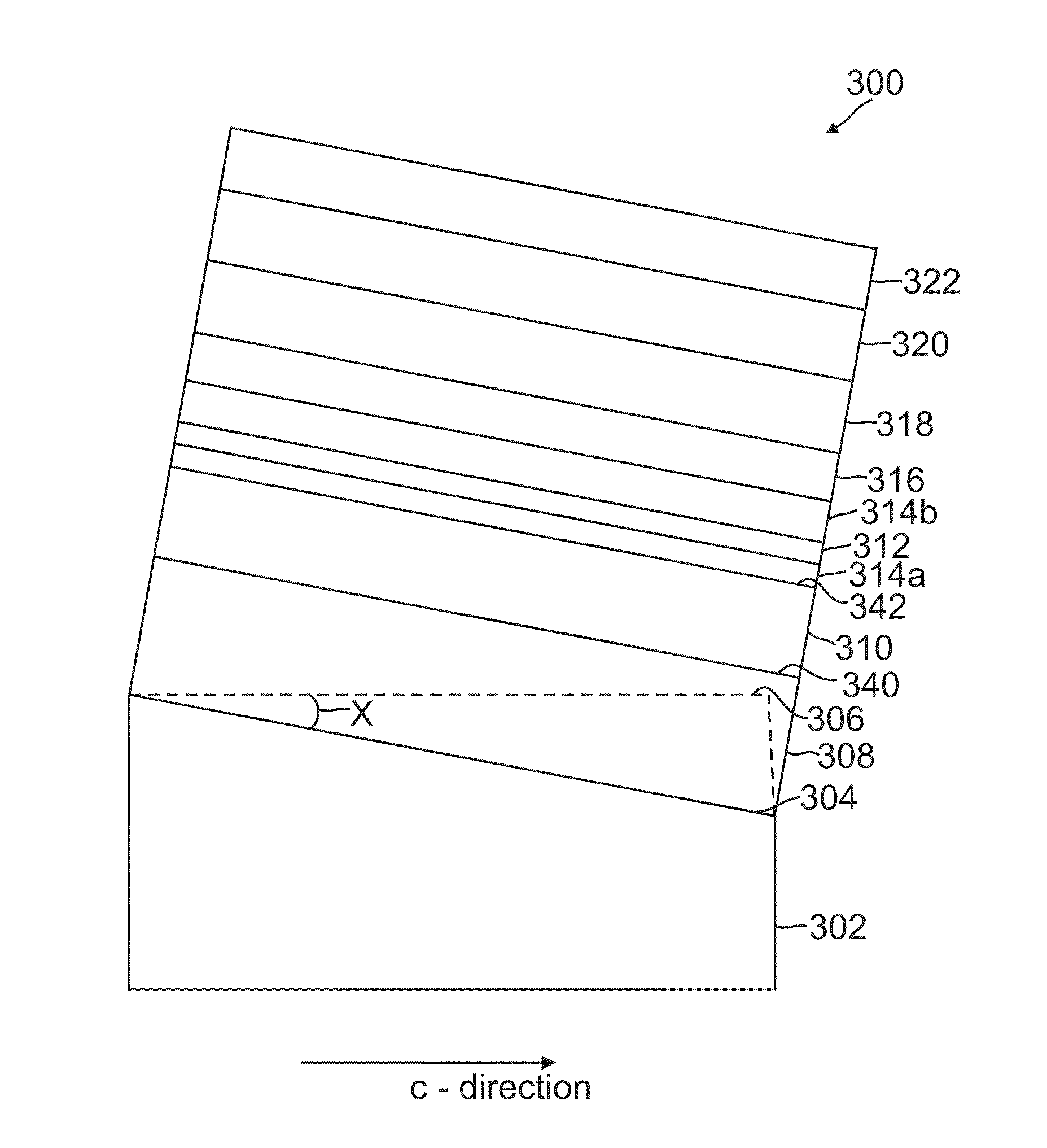
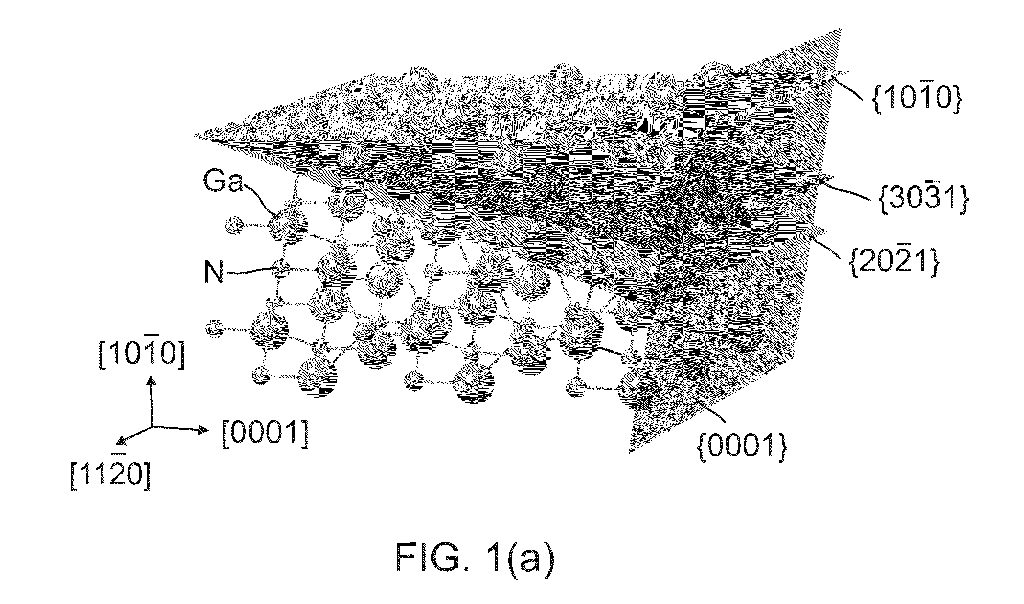
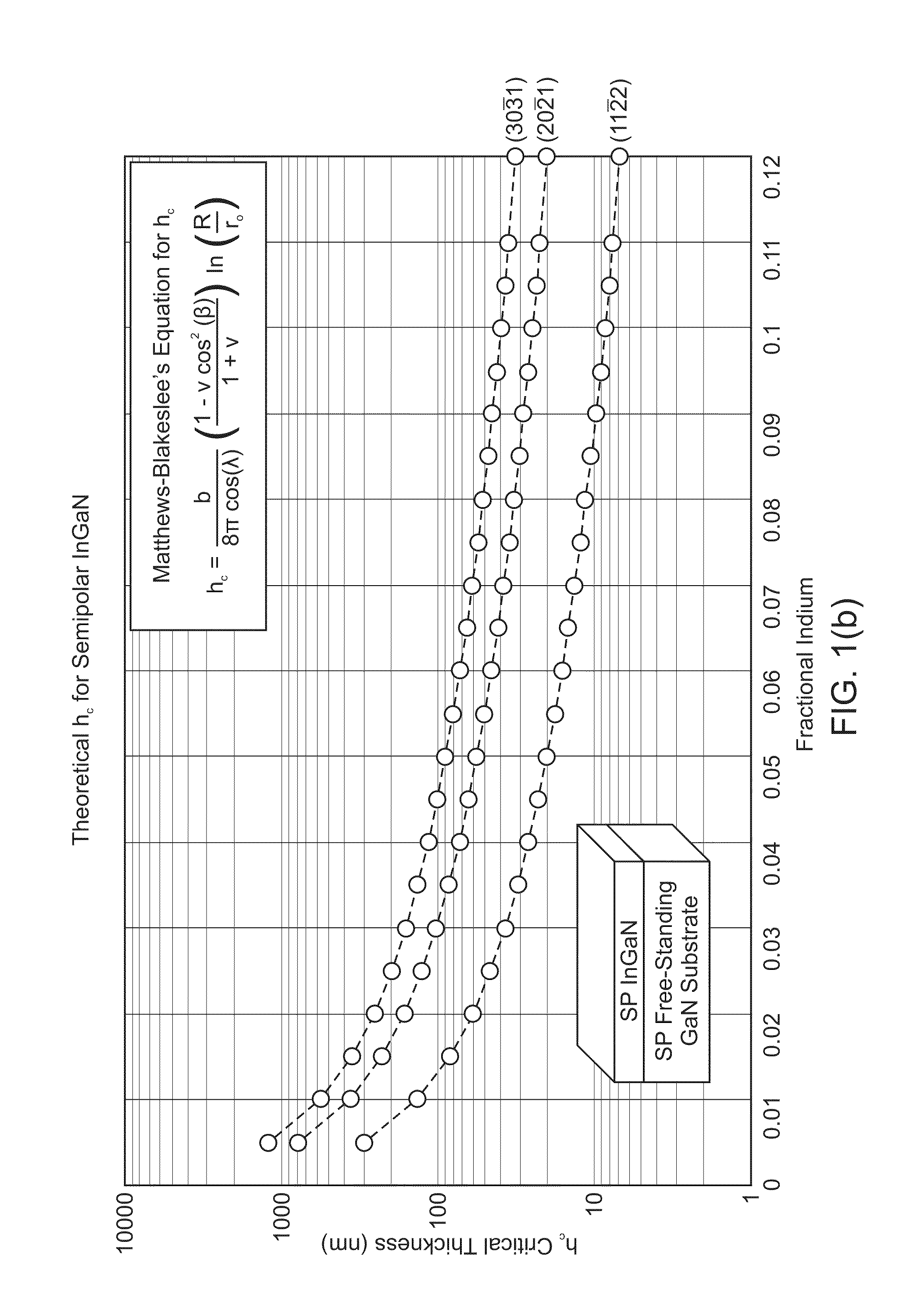
[0050](Al,Ga,In)N optoelectronic devices are grown on polar {0001}, non-polar {11-20} and {10-10}, and semi-polar {10-1-1}, {11-22} and {20-21} GaN crystal planes.

[0051]Lasers grown on polar and semi-polar planes suffer from polarization related electric fields in the quantum-wells that degrade device performance.

[0052]While non-polar {10-10} and {11-20} devices are free from polarization related effects, incorporation of high indium concentrations in {10-10} and high quality crystal growth of {11-20} devices have been shown to be difficult to achieve.

[0053]For example, suffic...


PUM


Abstract

An optoelectronic device grown on a miscut of GaN, wherein the miscut comprises a semi-polar GaN crystal plane (of the GaN) miscut x degrees from an m-plane of the GaN and in a c-direction of the GaN, where −15<x<−1 and 1<x<15 degrees.

Description

CROSS REFERENCE TO RELATED APPLICATIONS[0001]This application claims the benefit under 35 U.S.C. Section 119(e) of co-pending and commonly assigned U.S. Provisional Patent Application Ser. No. 61 / 310,638 filed on Mar. 4, 2010 by Po Shan Hsu, Kathryn M. Kelchner, Robert M. Farrell, Daniel Haeger, Hiroaki Ohta, Anurag Tyagi, Shuji Nakamura, Steven P. DenBaars, and James S. Speck, entitled “SEMI-POLAR III-NITRIDE OPTOELECTRONIC DEVICES ON M-PLANE SUBSTRATES WITH MISCUTS LESS THAN+ / −15 DEGREES IN THE C-DIRECTION,” attorney's docket number 30794.366 -US-P1 (2010-543-1);[0002]which application is incorporated by reference herein.[0003]This application is related to the following co-pending and commonly-assigned U.S. patent applications:[0004]U.S. Utility patent application Ser. No. 12 / 030,117, filed on Feb. 12, 2008, by Daniel F. Feezell, Mathew C. Schmidt, Kwang Choong Kim, Robert M. Farrell, Daniel A. Cohen, James S. Speck, Steven P. DenBaars, and Shuji Nakamura, entitled “Al(x)Ga(1-x)N...

Claims


Application Information

Patent Timeline
IPC IPC(8): H01S5/343H01L33/06H01L33/18
CPCB82Y20/00H01L21/02389H01L21/02433H01L21/0254H01L21/02609H01S5/0014H01S2304/04H01S5/22H01S5/3063H01S5/3202H01S5/3404H01S5/34333H01S5/2009H01S5/320275Y02E10/544H01S5/00H01S5/10H01S5/20H01L31/03044H01L31/036H01L31/0735H01L33/0025H01L33/0045H01L33/06H01L33/16H01L33/32H01S5/2031
Inventor HSU, PO SHANKELCHNER, KATHRYN M.FARRELL, ROBERT M.HAEGER, DANIEL A.OHTA, HIROAKITYAGI, ANURAGNAKAMURA, SHUJIDENBAARS, STEVEN P.SPECK, S. JAMES
Owner RGT UNIV OF CALIFORNIA
Why Eureka
Try Eureka