

Lead wire for solar cell, manufacturing method and storage method thereof, and solar cell
- Summary
- Abstract
- Description
- Claims
- Application Information
AI Technical Summary
Benefits of technology
Problems solved by technology
Method used
Image

Examples
example 1
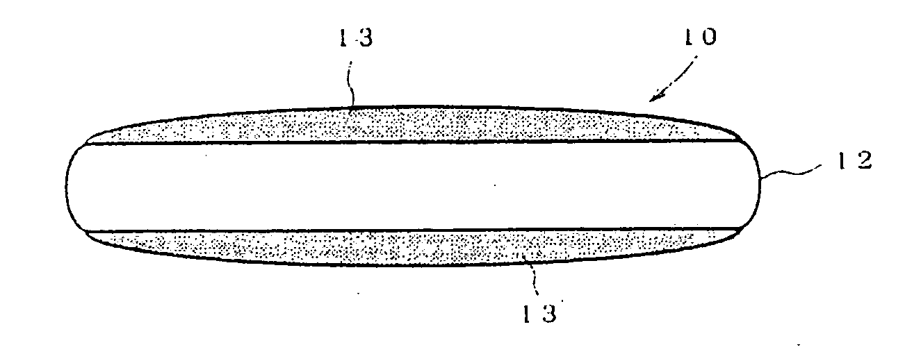
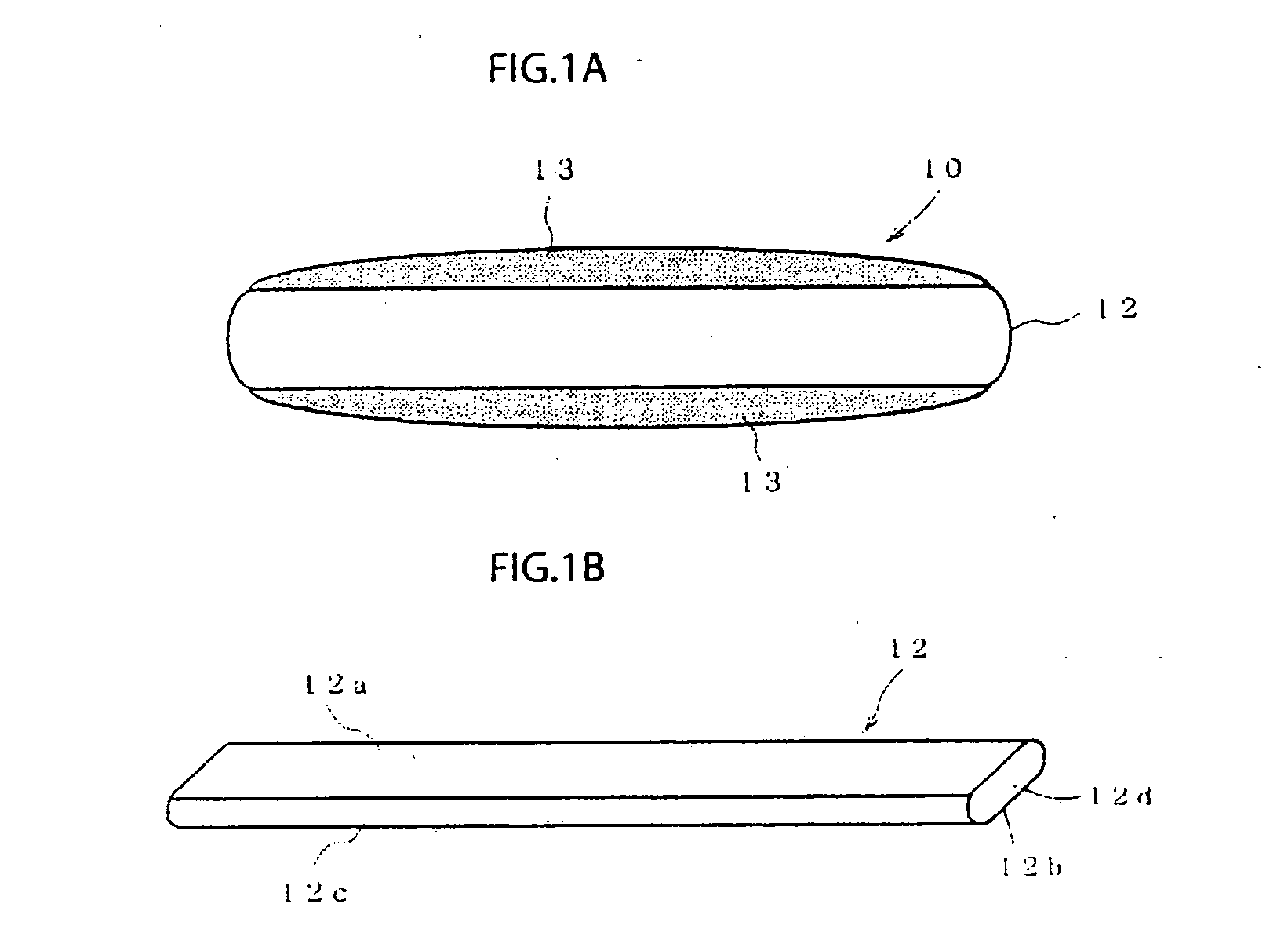
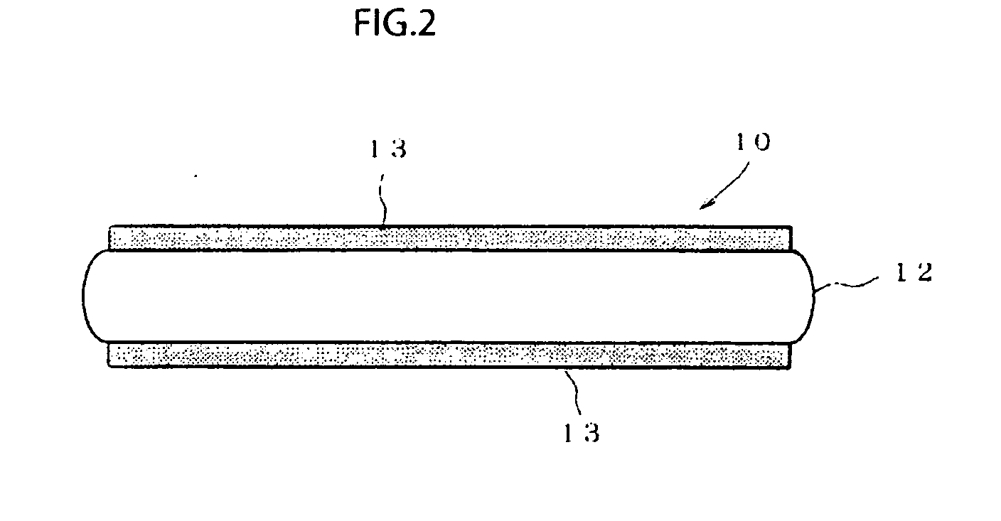
[0079]A Cu material as a raw conductive material was roll-processed, thereby forming a strip-shaped conductive material in a rectangular shape of 2.0 mm in width and 0.16 mm in thickness. The strip-shaped conductive material was heat-treated in a batch-type heating equipment, and further, Sn-3% Ag-0.5% Cu solder plating (liquidus-line temperature of 220° C.) was applied on the peripheral surface of the strip-shaped conductive material in the hot-dip plating equipment shown in FIG. 3 (at molten solder temperature of 340° C., workplace temperature of 30° C. and humidity in the workplace of 62 RH %), thereby forming a molten solder plated layer (a plating thickness is 20 μm at a middle portion) on upper and lower surfaces of the strip-shaped conductive material (a conductor is a heat-treated Cu). From the above, the solar cell lead wire of FIG. 1A was obtained. After that, oxide film thickness measurement (Auger analysis) and bonding strength measurement were immediately conducted.
examples 2 , 3 , 4 and 5
Examples 2, 3, 4 and 5
[0080]A strip-shaped conductive material was formed in the same manner as the solar cell lead wire 10 of Example 1, was heat-treated in a batch-type heating equipment, and further, Sn-3% Ag-0.5% Cu solder plating (liquidus-line temperature of 220° C.) was applied on the peripheral surface of the strip-shaped conductive material in the hot-dip plating equipment shown in FIG. 3 (at molten solder temperature of 340° C., workplace temperature of 30° C. and humidity in the workplace of 65 RH %), thereby forming a molten solder plated layer (a plating thickness is 20 μm at a middle portion) on upper and lower surfaces of the strip-shaped conductive material (a conductor is a heat-treated Cu). Furthermore, in Example 2, the manufactured solar cell lead wire was not packed and was stored in a constant temperature and humidity bath for 3 months under the conditions of 30° C.×65 RH %, and then, the oxide film thickness measurement (Auger analysis) and the bonding strengt...
examples 6 and 7
[0081]A strip-shaped conductive material was formed in the same manner as the solar cell lead wire 10 of Example 1, was heat-treated in a batch-type heating equipment, and further, Sn-3% Ag-0.5% Cu solder plating (liquidus-line temperature of 220° C.) was applied on the peripheral surface of the strip-shaped conductive material in the hot-dip plating equipment shown in FIG. 3 (at molten solder temperature of 340° C., workplace temperature of 20° C. and humidity in the workplace of 50 RH % in Example 6, and at molten solder temperature of 340° C., workplace temperature of 30° C. and humidity in the workplace of 65 RH % in Example 7), thereby forming a molten solder plated layer (a plating thickness is 20 μm at a middle portion) on upper and lower surfaces of the strip-shaped conductive material (a conductor is a heat-treated Cu). Furthermore, in Example 6, after making the solar cell lead wire, the oxide film thickness measurement (Auger analysis) and the bonding strength measurement...
PUM
| Property | Measurement | Unit |
|---|---|---|
| Temperature | aaaaa | aaaaa |
| Temperature | aaaaa | aaaaa |
| Fraction | aaaaa | aaaaa |
Abstract
Description
Claims
Application Information