

Method and Device Utilizing Strained AZO Layer and Interfacial Fermi Level Pinning in Bifacial Thin Film PV Cells
a thin film photovoltaic cell and interfacial fermi level technology, applied in semiconductor/solid-state device manufacturing, semiconductor devices, electrical equipment, etc., to achieve the effect of reducing internal electric field strength, reducing barrier, and reducing electric field strength
- Summary
- Abstract
- Description
- Claims
- Application Information
AI Technical Summary
Benefits of technology
Problems solved by technology
Method used
Image

Examples
Embodiment Construction
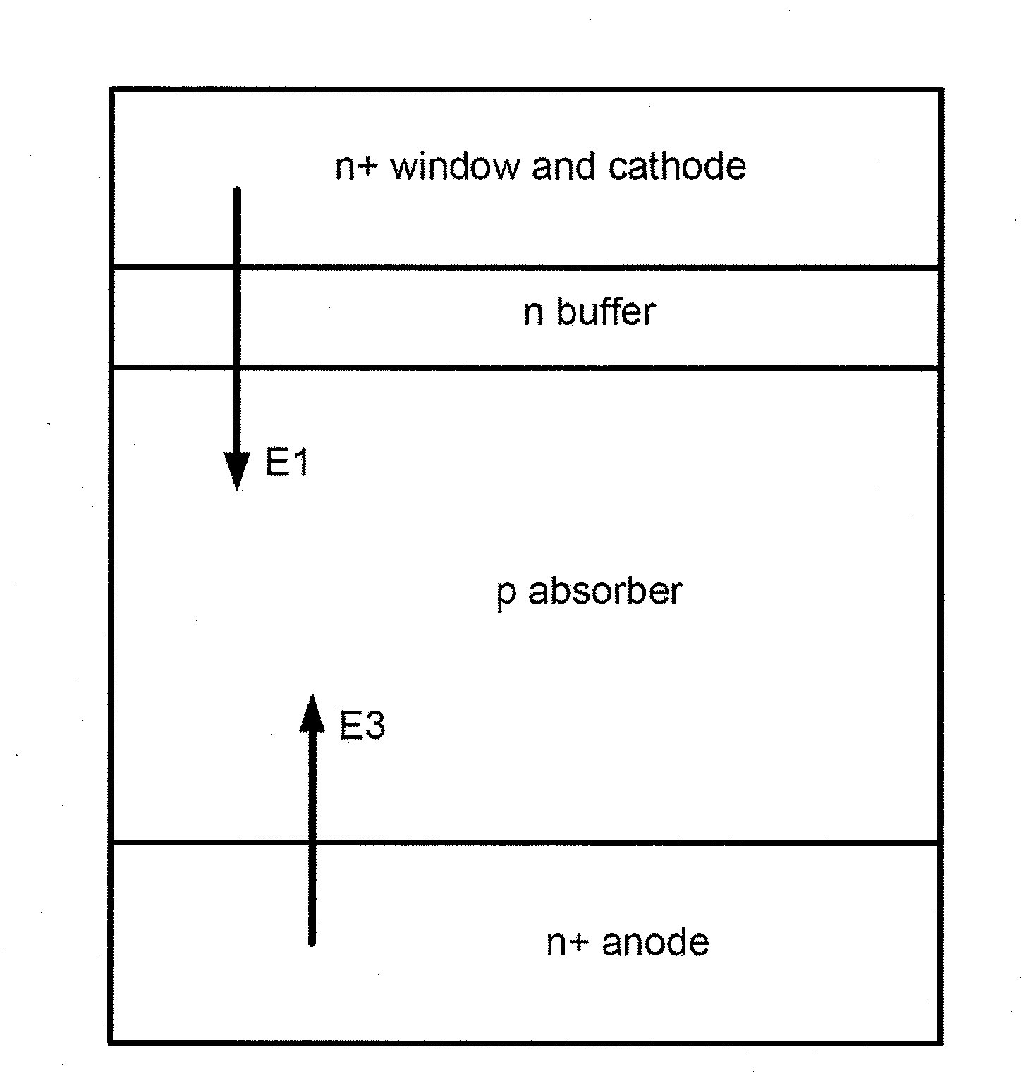
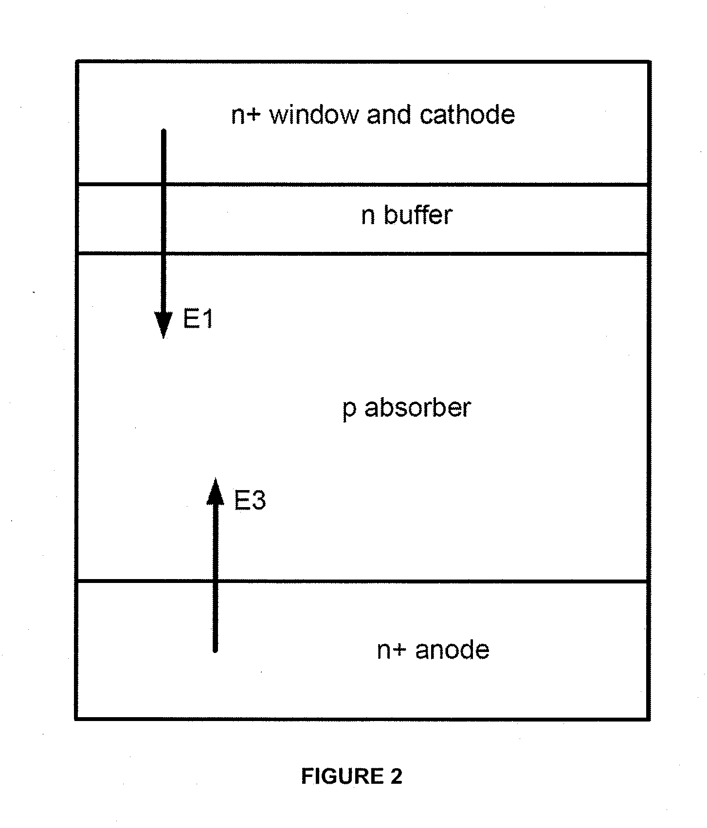
[0019]Embodiments of the present invention provide a method and device structure for a bifacial thin film photovoltaic cell. They include a method for forming a bifacial thin film photovoltaic device utilizing a strain field in the anode layer and interface Fermi level pinning to modify the internal electric field at the anode-absorber interface, enhancing cell efficiency. A device utilizing an AZO layer as an interface between a PV absorber and an anode layer for enhancing hole collection is provided.
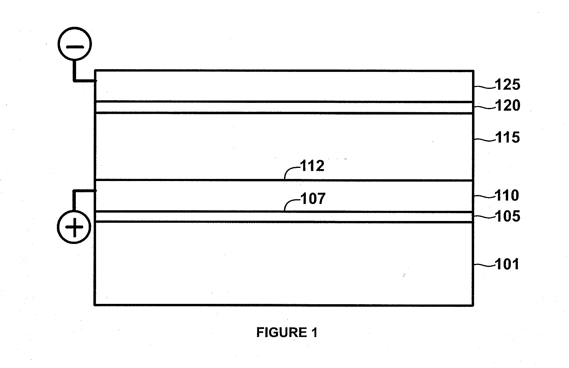
[0020]FIG. 1 is a diagram illustrating a thin film photovoltaic cell utilizing an aluminum doped zinc oxide layer at anode-absorber interface according to an embodiment of the present invention. As shown, a thin film photovoltaic (PV) cell 100 is formed on a substrate 101. Typically, for bifacial thin film PV cell a transparent material, e.g. soda lime glass, is selected for the substrate. In an embodiment, an intermediate layer 105 is formed overlying a surface region of the substrate...
PUM
 Abstract
Description
Claims
Application Information