

Liquid crystal display device
a liquid crystal display and display device technology, applied in static indicating devices, instruments, transportation and packaging, etc., can solve the problems of display defects, unwanted shavings on the surface of alignment films formed, etc., and achieve the effect of high sensitivity
- Summary
- Abstract
- Description
- Claims
- Application Information
AI Technical Summary
Benefits of technology
Problems solved by technology
Method used
Image

Examples
example 1
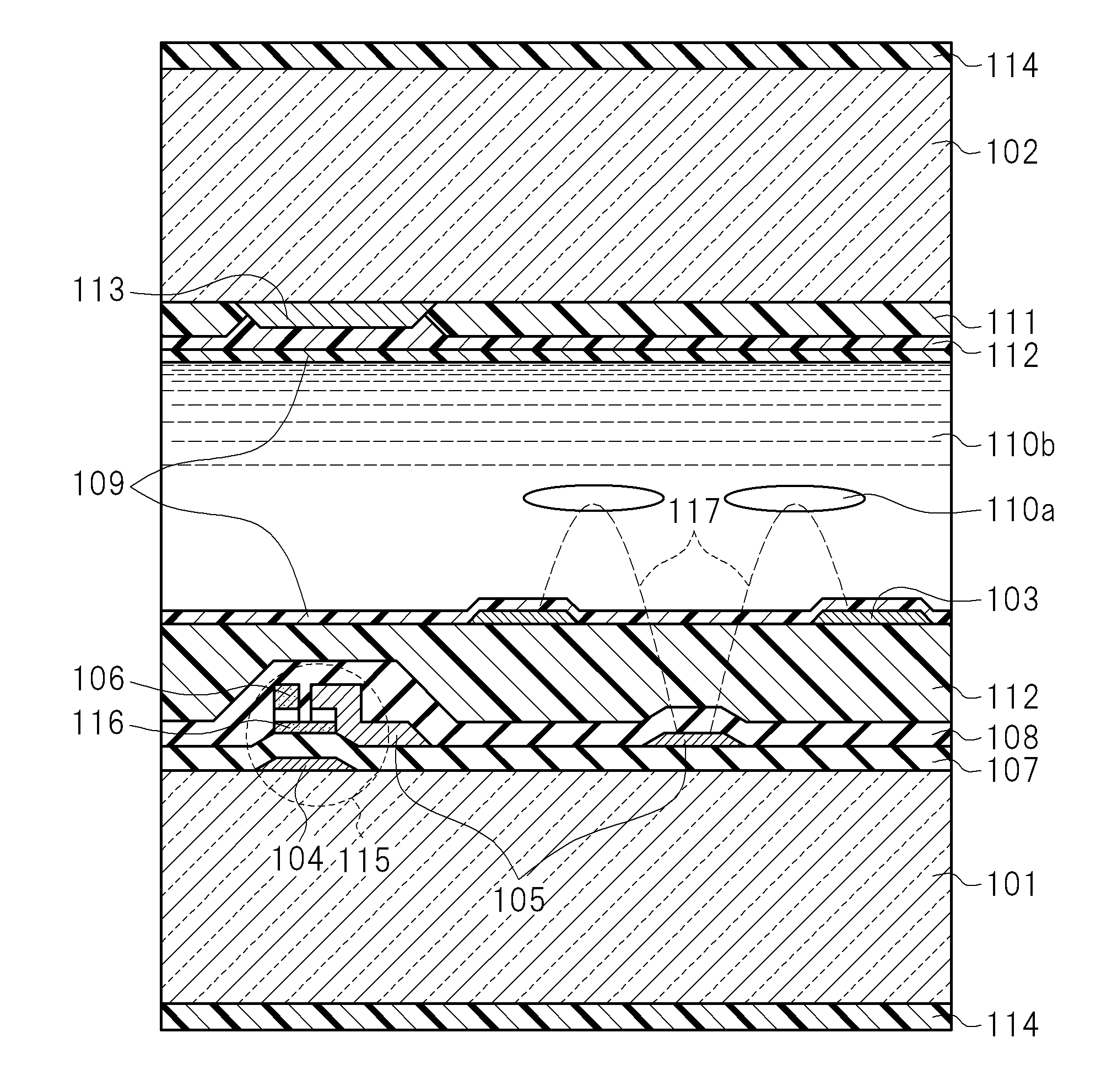
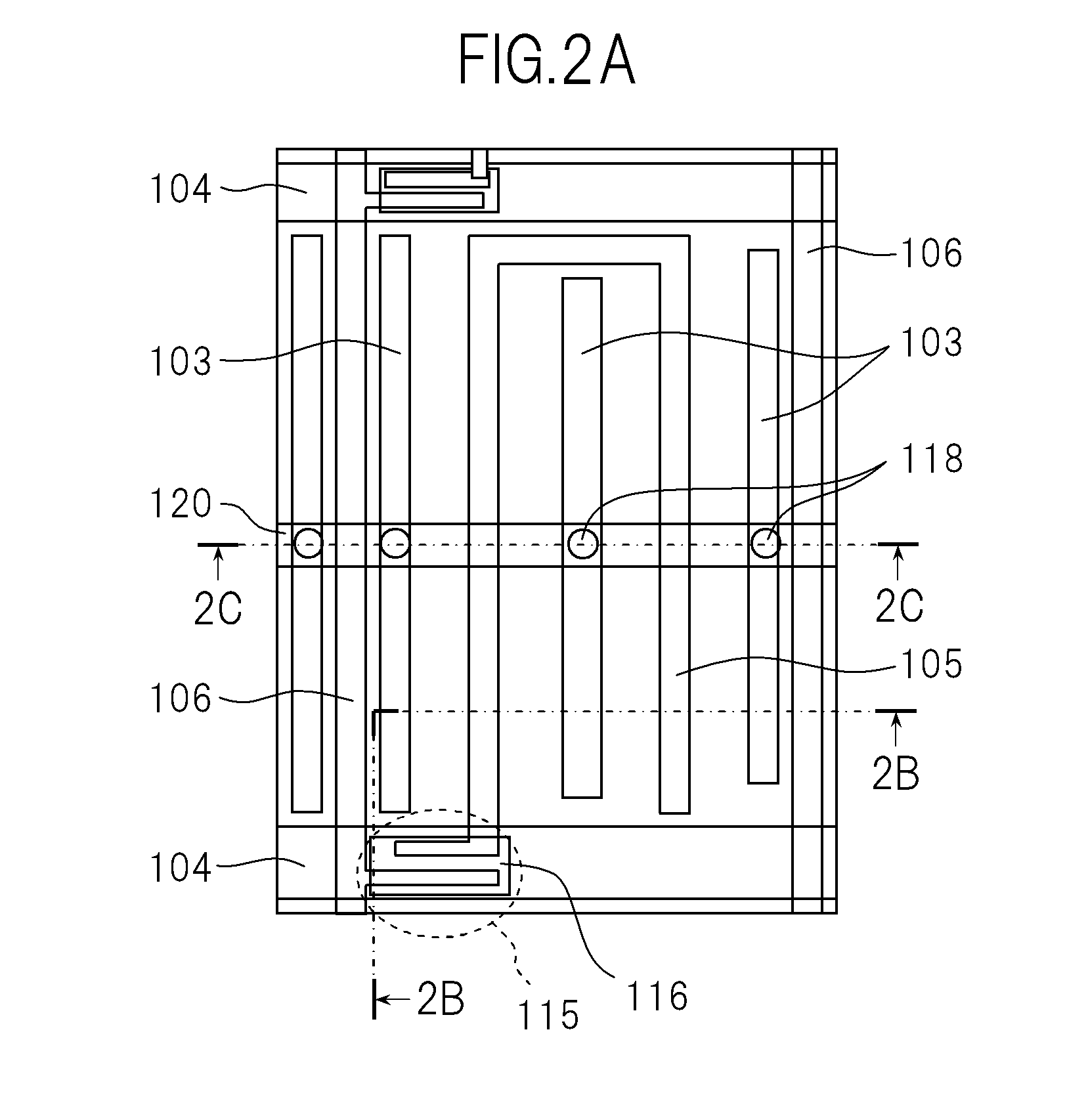
[0078]FIG. 1 is a schematic cross-sectional view in the vicinity of one pixel of a liquid crystal display device according to Example 1. Further, FIG. 2A is a schematic plan view of an active matrix substrate illustrating a configuration in the vicinity of one pixel of the liquid crystal display device according to Example 1. FIG. 2B is a cross-sectional view taken along the line 2B of FIG. 2A. FIG. 2C is a cross-sectional view taken along the line 2C of FIG. 2A. Further, FIG. 1 corresponds to apart of the cross-section taken along the line 2B of FIG. 2A.
[0079]FIGS. 2B and 2C emphasize and schematically illustrate configurations of main portions, and do not correspond one by one to cut portions of the line 2B and the line 2C in FIG. 2A. For example, a semiconductor film 116 is not illustrated in FIG. 2B, and only one through-hole 118 that connects each common electrode 103 and a common line 120 is representatively illustrated in FIG. 2C.
[0080]In this example, scanning lines (gate el...
example 2
[0112]FIG. 3 is a schematic cross-sectional view illustrating a vicinity of one pixel in the liquid crystal display device according to Example 2. FIG. 4A is a schematic plan view of an active matrix substrate illustrating the configuration of the vicinity of one pixel of the liquid crystal display device according to Example 2. FIG. 4B is a cross-sectional view taken along the line 4B illustrated in FIG. 4A. FIG. 4C is a cross-sectional view taken along the line 4C illustrated in FIG. 4A.
[0113]Further, FIG. 4 is a schematic view of an active matrix substrate illustrating a configuration in the vicinity of one pixel of the liquid crystal display device according to this example. FIG. 4A is a plan view, FIG. 4B is a cross-sectional view taken along the line 4B of FIG. 4A, and FIG. 4C is a cross-sectional view taken along the line 4C of FIG. 4A. Further, FIG. 3 corresponds to a part of the cross-section taken along the line 4B of FIG. 4A.
[0114]FIGS. 4B and 4C emphasize and schematical...
example 3
[0133]FIG. 5 is a schematic cross-sectional view of the vicinity of one pixel in a liquid crystal display device according to Example 3. In the figure, the same symbols as those in the figures of the respective examples correspond to identical function portions. As illustrated in FIG. 5, in this example, the pixel electrode 105 disposed below the protective insulating film 108 is pulled up onto the organic protective film 112 through the through-hole 118 so as to be arranged in the same layer as that of the common electrode 103. In this configuration, a voltage for driving the liquid crystal can be further reduced.
[0134]In the TFT liquid crystal display device configured as described above, at the time of applying no electric field, the liquid crystal molecules 110a forming the liquid crystal composition layer 110b are aligned substantially in parallel to the surfaces of the glass substrates 101 and 102 which face each other. The liquid crystal molecules 110a are homogeneously align...
PUM
| Property | Measurement | Unit |
|---|---|---|
| pretilt angle | aaaaa | aaaaa |
| thickness | aaaaa | aaaaa |
| thicknesses | aaaaa | aaaaa |
Abstract
Description
Claims
Application Information