Low overhead and timing improved architecture for performing error checking and correction for memories and buses in system-on-chips, and other circuits, systems and processes

a memory and bus technology, applied in the field of low overhead and timing improved architecture, can solve the problems of slowing down the operating frequency of the system in which the memory is used, affecting throughput, and other types of access to memory are handled inefficiently

Active Publication Date: 2011-09-15
TEXAS INSTR INC
View PDF12 Cites 67 Cited by
  • Summary
  • Abstract
  • Description
  • Claims
  • Application Information

AI Technical Summary

Benefits of technology

[0008]Generally, a form of the invention involves an electronic circuit for use with an accessing circuit that supplies a given address and a partial write data portion and also has dummy cycles. The electronic circuit includes a memory circuit accessible at addresses, an address buffer, a data buffer coupled to the memory circuit, and a control circuit operable in the dummy cycles to read data from the memory circuit to the data buffer from a next address location in the

Problems solved by technology

Conventional error correction codes can be used to encode the data in the memory; however, they are associated with the following limitations and problems:
(i) Implementations using Error Checking and Correction (ECC) schemes based on Hamming codes are associated with a higher timing overhead, which slows down the operating frequency of the

Method used


Image

  • Low overhead and timing improved architecture for performing error checking and correction for memories and buses in system-on-chips, and other circuits, systems and processes
  • Low overhead and timing improved architecture for performing error checking and correction for memories and buses in system-on-chips, and other circuits, systems and processes
  • Low overhead and timing improved architecture for performing error checking and correction for memories and buses in system-on-chips, and other circuits, systems and processes

Examples


Embodiment Construction

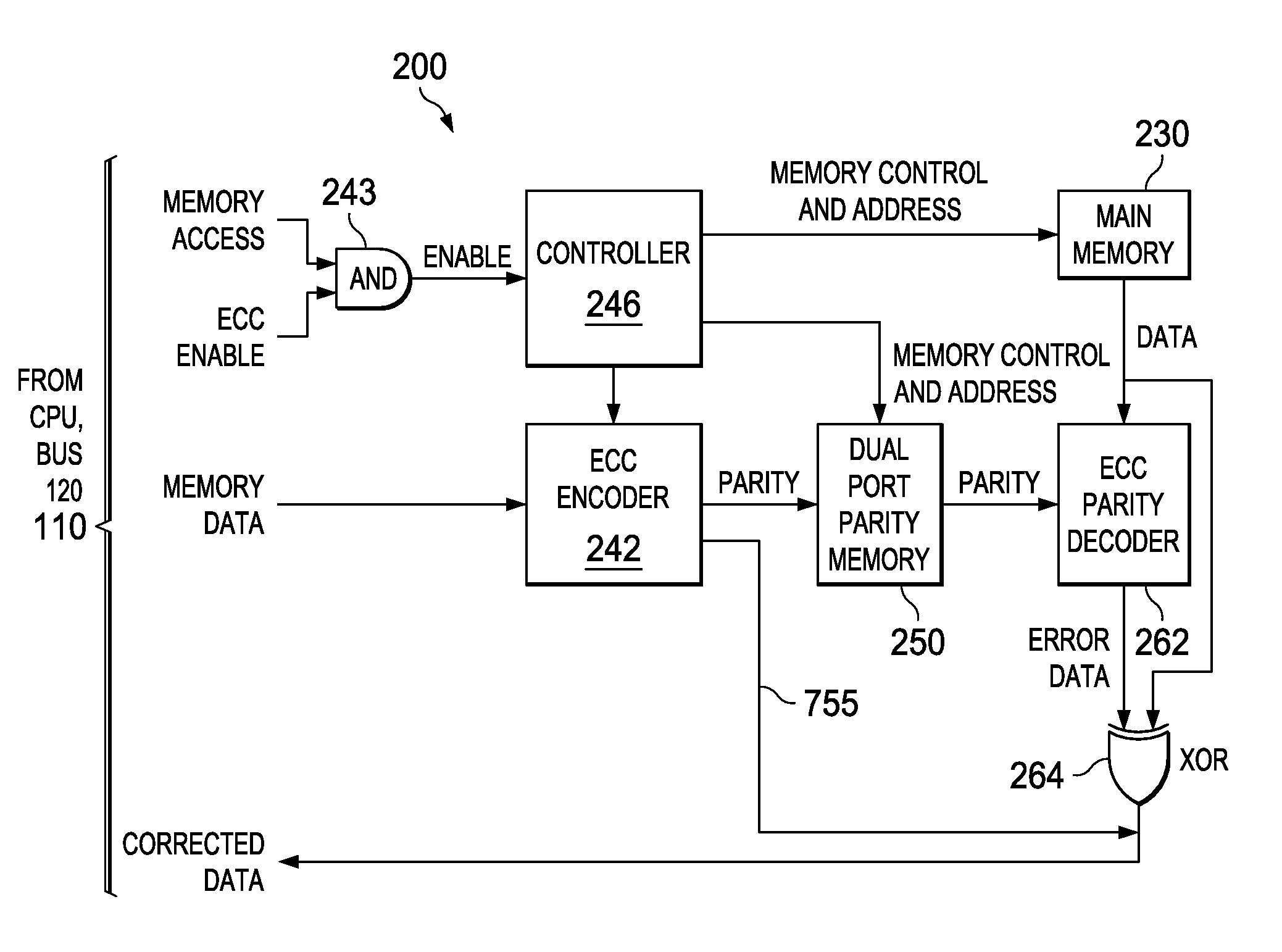
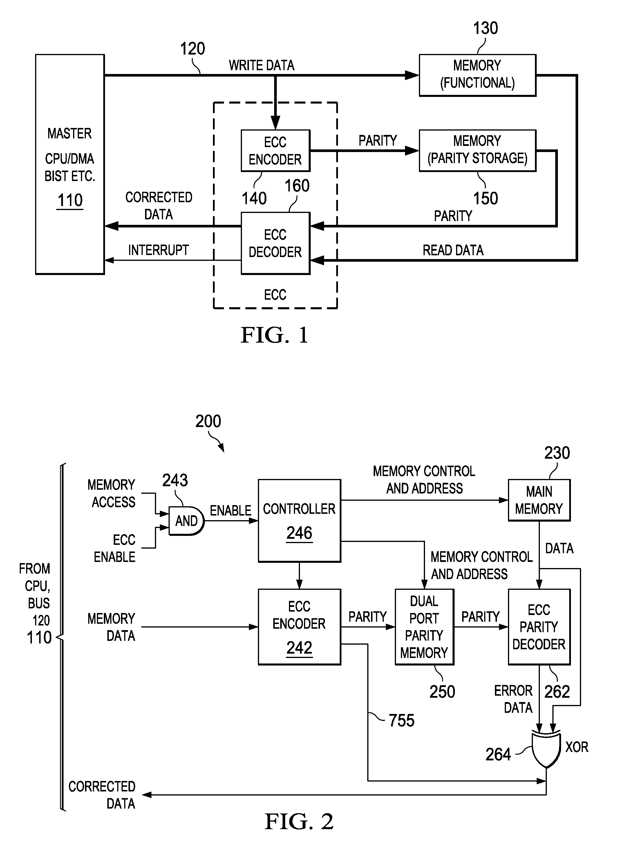
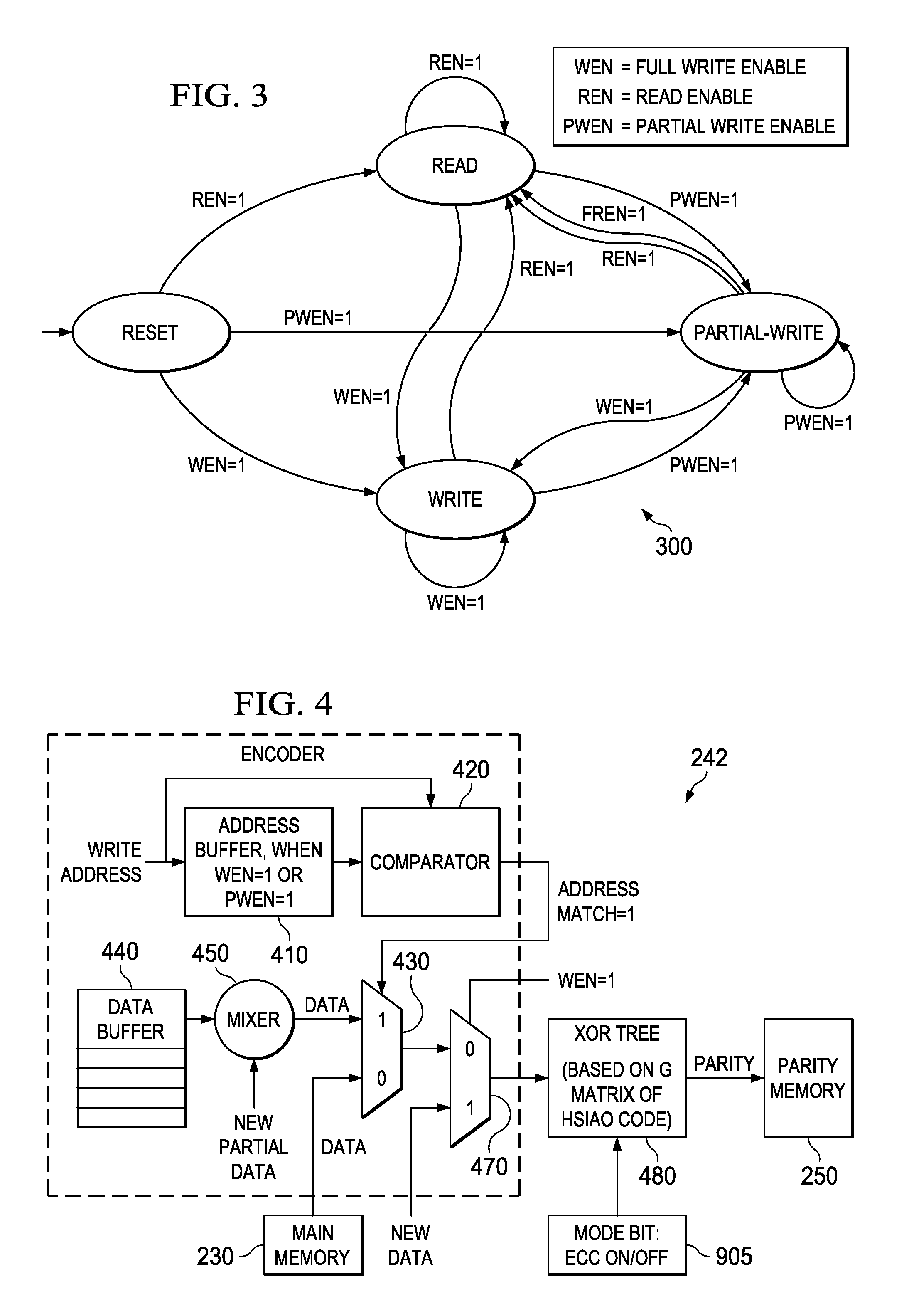
[0047]To solve these problems and others, a high performance ECC embodiment is realized through remarkable controller structures and operations and provision of local buffering in the encoder / decoder. The embodiments provide throughput improvement for partial writes exploiting locality in data traffic, and also provide throughput improvement for pipelined ECC with pipeline-unaware CPUs. Some embodiments take advantage of the locality characteristic of data traffic in applications to significantly reduce cycle overhead of partial word operations, which in-turn increases the throughput. Some read embodiments enhance throughput by read bypass from a local write buffer to read output and also take advantage of locality in data traffic. Further, some of the embodiments provide an architecture that uses Hsiao codes to realize low area and low timing overhead encoders and decoders individually and in combinations.

[0048]Test process embodiments are disclosed for using the structural embodim...


PUM


Abstract

An electronic circuit (200) for use with an accessing circuit (110) that supplies a given address and a partial write data portion and also has dummy cycles. The electronic circuit (200) includes a memory circuit (230) accessible at addresses, an address buffer (410), a data buffer (440) coupled to the memory circuit (230), and a control circuit (246) operable in the dummy cycles to read data from the memory circuit (230) to the data buffer (440) from a next address location in the memory circuit (230) and to store that next address in the address buffer (410). The electronic circuit further includes a multiplexer (430), a comparing circuit (420) responsive to the given address and a stored address in the address buffer (410), to operate the multiplexer (430) to pass data from the data buffer (440) or to pass data from the memory circuit (230) instead; and a mixer circuit (450) operable to put the partial write data portion into the data taken from the selected one of the data buffer (440) or memory circuit (230). Other circuits, devices, systems, processes of operation and processes of manufacture are also disclosed.

Description

CROSS-REFERENCES TO RELATED APPLICATIONS[0001]This application is related to India Patent Application 667 / CHE / 2010 “A Low Overhead and Timing Improved Architecture for Performing Error Checking and Correction for Memories and Buses in System-On-Chips, Systems and Processes,” filed Mar. 12, 2010, for which priority is claimed under the Paris Convention and 35 U.S.C. 119 and all other applicable law, and which is incorporated herein by reference in its entirety.STATEMENT REGARDING FEDERALLY SPONSORED RESEARCH OR DEVELOPMENT[0002]Not applicable.COPYRIGHT NOTIFICATION[0003]Portions of this patent application contain materials that are subject to copyright protection. The copyright owner has no objection to the facsimile reproduction by anyone of the patent document, or the patent disclosure, as it appears in the United States Patent and Trademark Office, but otherwise reserves all copyright rights whatsoever.BACKGROUND[0004]Permanent failures in a memory due to effects such as aging, an...

Claims


Application Information

Patent Timeline
IPC IPC(8): G11C8/06H03M13/05G06F11/10
CPCG06F11/1052G11C8/06G11C8/16G06F11/1008G11C29/42G11C2029/0411H03M13/19
Inventor KUMAR, SANJAYDUTTA, AMIT KUMARPAREKHJI, RUBIN A.RAVI, SRIVATHS
Owner TEXAS INSTR INC
Why Eureka
Try Eureka