Photoelectric conversion film-stacked solid-state imaging device without microlenses, its manufacturing method, and imaging apparatus

a technology of solid-state imaging and photoelectric conversion, which is applied in the manufacturing of semiconductor/solid-state devices, electrical devices, semiconductor devices, etc., can solve the problems of low reliability of adhesives, affecting the mass-productivity and reliability of adhesives, and increasing the cost of adhesives, so as to increase the reliability of imaging apparatus, miniaturize and increase mass-productivity. the effect of reliability

Inactive Publication Date: 2011-09-22
FUJIFILM CORP
View PDF5 Cites 11 Cited by
  • Summary
  • Abstract
  • Description
  • Claims
  • Application Information

AI Technical Summary

Benefits of technology

[0013]The invention makes it possible to provide a compact and thin solid-state imaging device in which no gaps need to be formed between a transparent substrate and an imaging device chip because of absence of microlenses, which enables use of a transparent adhesive whose refractive index is not subjected to any restrictions, and which has such a device structure as to be high in mass-productivity and reliability. Furthermore, the invention may miniaturize and increase the reliability of an imaging apparatus incorporating such a solid-state imaging device.

Problems solved by technology

However, there are some problems relating to the material of the adhesive.
Furthermore, the reliability of the adhesive is low unless it is made of a material having a small water absorption coefficient.
Required to be small in refractive index and water absorption coefficient, the material of the adhesive needs to be selected from only a small number of options, resulting in a problem of cost increase.
However, a manufacturing step of forming gaps is complex and hence is a factor of manufacturing cost increase.
There is another problem that the gaps make it difficult to reduce the thickness of the solid-state imaging device.

Method used


Image

  • Photoelectric conversion film-stacked solid-state imaging device without microlenses, its manufacturing method, and imaging apparatus
  • Photoelectric conversion film-stacked solid-state imaging device without microlenses, its manufacturing method, and imaging apparatus
  • Photoelectric conversion film-stacked solid-state imaging device without microlenses, its manufacturing method, and imaging apparatus

Examples


Embodiment Construction

[0023]An embodiment of the present invention will be hereinafter described with reference to the drawings.

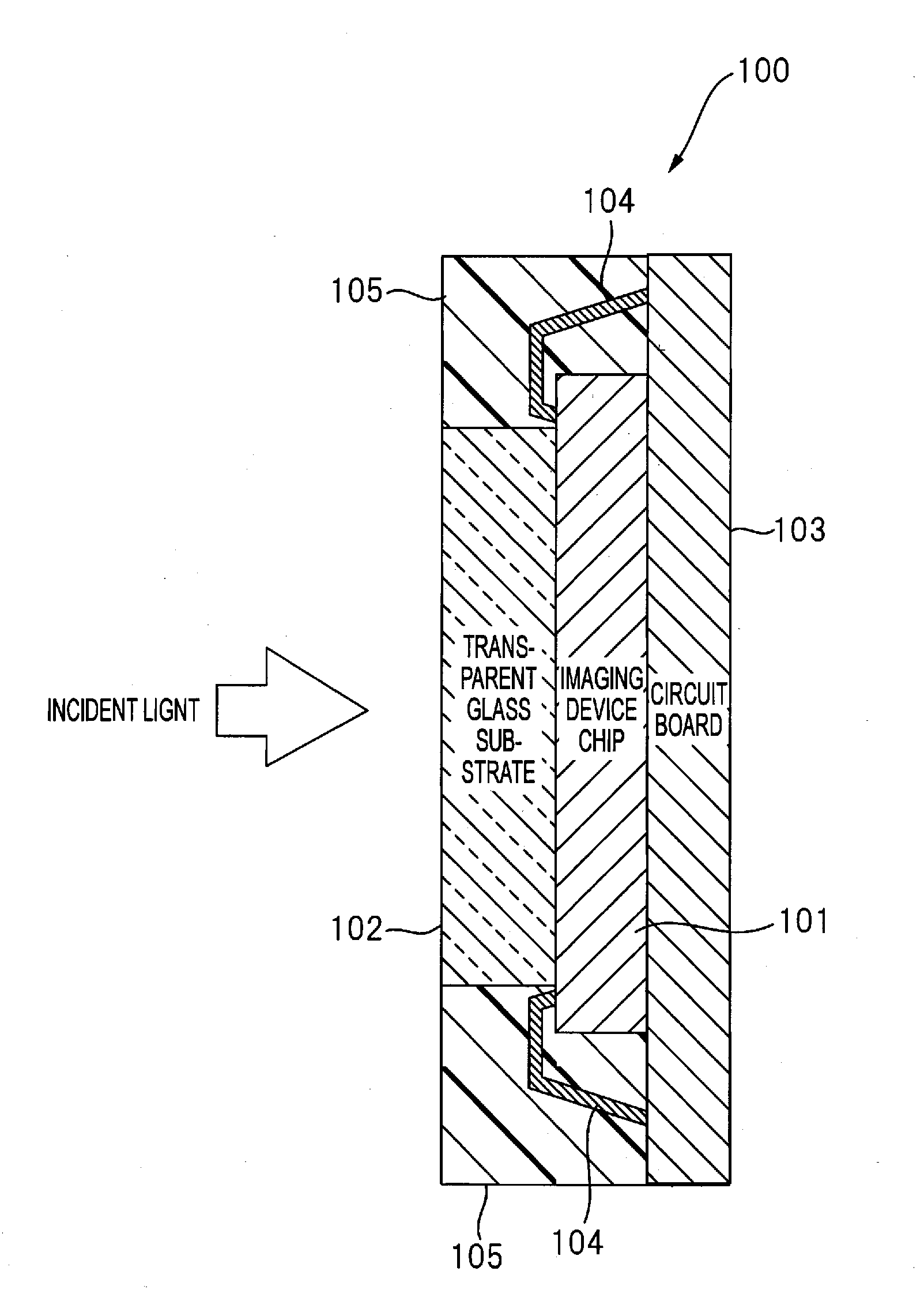
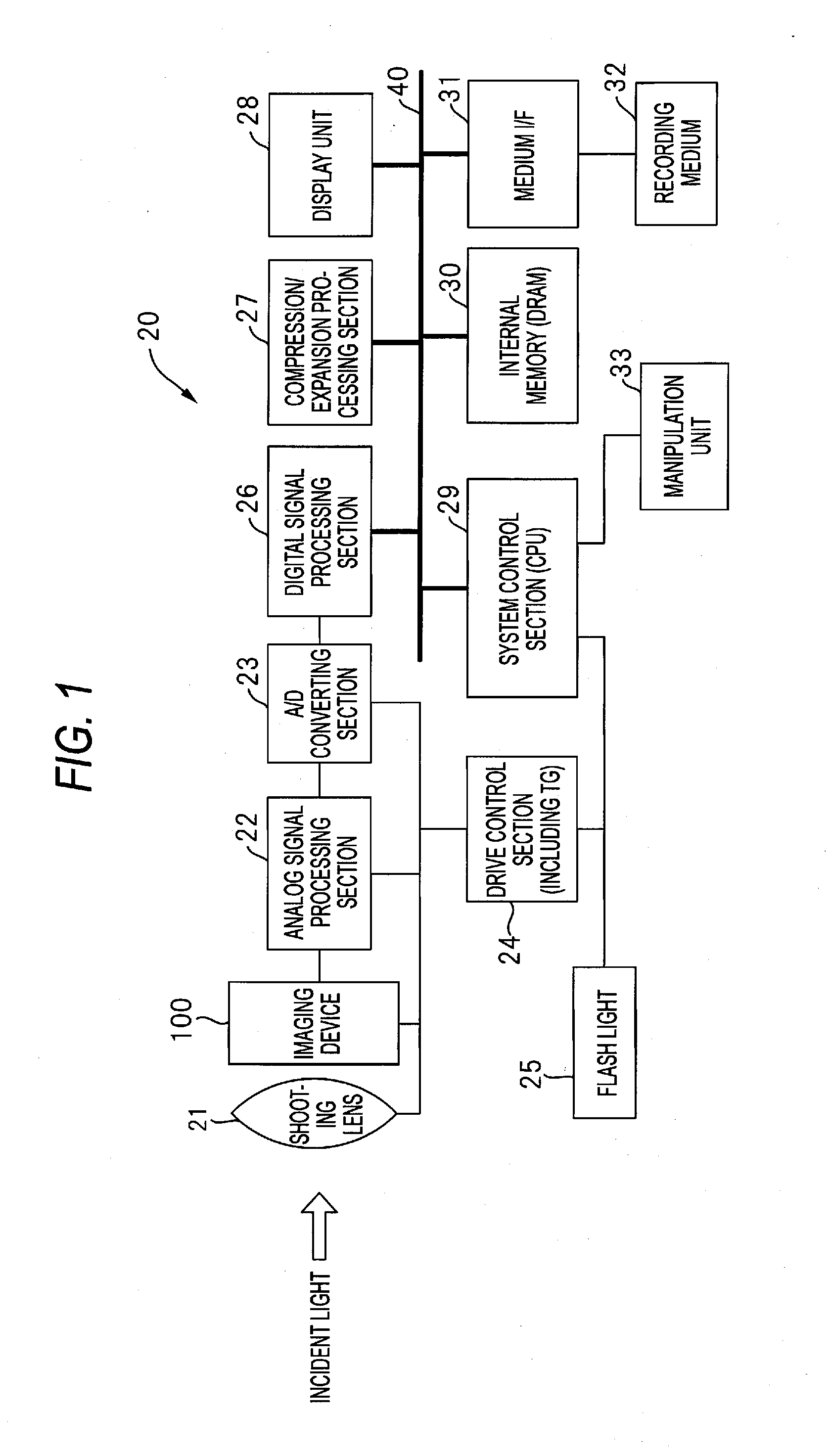
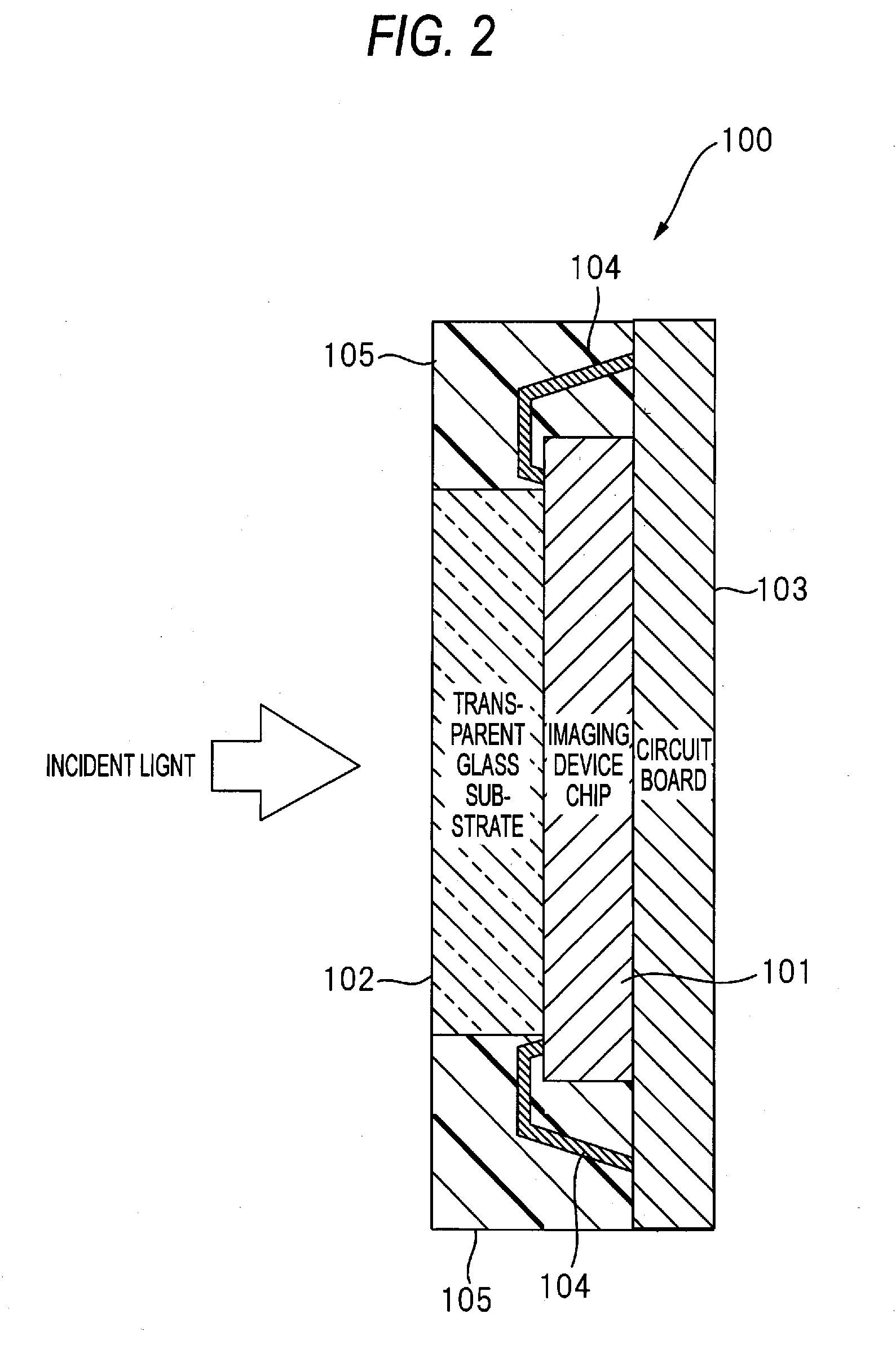
[0024]FIG. 1 is a block diagram showing the configuration of a digital camera (imaging apparatus) 20 according to the embodiment of the invention. The digital camera 20 is equipped with a solid-state imaging device 100, a shooting lens 21, an analog signal processing section 22 which performs analog processing such as automatic gain control (AGC) and correlated double sampling on analog image data that is output from the solid-state imaging device 100, an analog-to-digital (A / D) converting section 23 which converts analog image data that is output from the analog signal processing section 22 into digital image data, a drive control section (including a timing generator) 24 which drive-controls the shooting lens 21, the A / D-converting section 23, the analog signal processing section 22, and the solid-state imaging device 100 according to an instruction from a system control secti...


PUM


Abstract

There are provided a circuit board; a semiconductor substrate bonded to a light-incidence-side surface of the circuit board; a photoelectric conversion film stacked on a layer that is disposed on the light incidence side of the semiconductor substrate; an imaging device chip having signal reading means which is formed in a surface portion of the semiconductor substrate, for reading out, as shot image signals, signals corresponding to signal charge amounts detected by the photoelectric conversion film according to incident light quantities; a transparent substrate bonded to a layer that is disposed on the light incidence side of the photoelectric conversion film with a transparent resin adhesive; and bonding wires which connect connection pads formed on a peripheral portion, not covered with the transparent substrate, of the semiconductor substrate to connection terminals on the circuit board.

Description

[0001]The present application claims priority from Japanese Patent Application No. 2010-061620 filed on Mar. 17, 2010, the entire content of which is incorporated herein by reference.BACKGROUND OF INVENTION[0002]1. Field of the Invention[0003]The present invention relates to a solid-state imaging device incorporated in an imaging apparatus such as a digital camera. More particularly, the invention relates to a photoelectric conversion film-stacked solid-state imaging device that is configured so as to be suitable for use in an imaging apparatus, as well as its manufacturing method.[0004]2. Description of the Related Art[0005]Solid-state imaging devices have a soft surface because its photodetecting surface is provided with microlenses (top lenses) made of resin or the like and a color filter layer. Therefore, it is necessary to protect the photodetecting surface to prevent formation of scratches and sticking of dust etc. To this end, a transparent substrate such as a glass substrate...

Claims


Application Information

Patent Timeline
Patent Type & Authority Applications(United States)
IPC IPC(8): H01L31/0224H01L31/18H01L31/0232
CPCH01L27/14618H01L27/14683H01L27/14627H01L24/97H01L2224/48091H01L2224/48095H01L2224/48227H01L2224/83192H01L2224/92247H01L2924/15788H01L2924/181H01L2924/1815H01L2924/00014H01L2924/00H01L2924/00012
Inventor INOMATA, HIROSHIWATANABE, EIJI
Owner FUJIFILM CORP
Why Eureka
Try Eureka