
Surface plasmon enhanced light-emitting diode

Inactive Publication Date: 2011-09-29
NAT CHENG KUNG UNIV
View PDF1 Cites 16 Cited by
  • Summary
  • Abstract
  • Description
  • Claims
  • Application Information

AI Technical Summary

Benefits of technology

[0009]Therefore, an object of the present invention is to provide a surface plasmon enhanced light-emitting diode, in which the epitaxial layers can be formed in a good quality, in which the effective areas that are not blocked by metal nanostructures on a p-type semiconductor layer can be increased, and in which the light-emitting efficiency can be improved.

Problems solved by technology

Furthermore, in practice, the quantity of Ag nanoparticles in the Ag nanoparticle layer is insufficient to form a continuous layer.
Accordingly, the Ag nanoparticle layer is uneven, and the quality of the epitaxial layers that are formed above the heterogeneous material (Ag) is relatively poor.
Thus, in this case, it is likely to adversely affect the light-emitting efficiency of the LED.
However, an effective area on the p-GaN layer for light emitting from a light-emitting layer is blocked and limited by the high density of the Ag nano-island structures.
In this case, the p-GaN layer of 60 nm is insufficient for maintaining the sufficient width of the depletion region required for a well-operated LED.

Method used


Image

  • Surface plasmon enhanced light-emitting diode
  • Surface plasmon enhanced light-emitting diode
  • Surface plasmon enhanced light-emitting diode

Examples


Embodiment Construction

[0016]Before the present invention is described in greater detail with reference to the accompanying preferred embodiments, it should be noted herein that like elements are denoted by the same reference numerals throughout the disclosure.

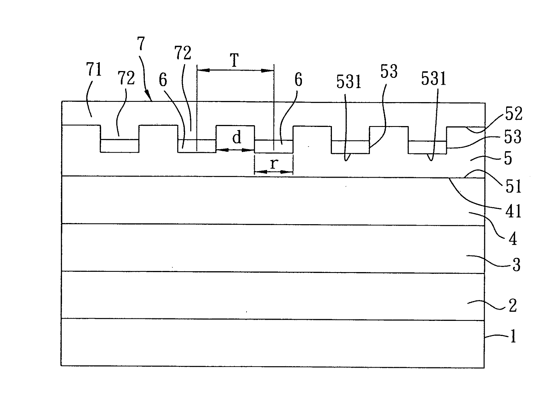
[0017]Referring to FIG. 1, a surface plasmon enhanced light-emitting diode (LED) of the first preferred embodiment of the present invention includes, from bottom to top, a substrate 1, a nucleation layer 2, an n-type semiconductor layer 3, a light-emitting layer 4, a p-type semiconductor layer 5, a plurality of metal filler elements 6, and an electrode-contacting layer 7.

[0018]In this preferred embodiment, the substrate 1 is a sapphire substrate (Al2O3), and the nucleation layer 2 is made of a GaN material and covers a surface of the substrate 1. The n-type semiconductor layer 3 is made of an n-doped GaN material, and covers a surface of the nucleation layer 2. The light-emitting layer 4 has an upper surface 41, facing the p-type semiconductor layer...


PUM


Abstract

A surface plasmon enhanced light-emitting diode includes, from bottom to top, a substrate, an n-type semiconductor layer, a light-emitting layer, a p-type semiconductor layer, and a plurality of metal filler elements. The p-type semiconductor layer includes upper and lower surfaces, and the upper surface is recessed downward to form a plurality of spaced apart recesses for receiving the metal filler elements, respectively.

Description

CROSS-REFERENCE TO RELATED APPLICATION[0001]This application claims priority of Taiwanese application no. 099108687, filed on Mar. 24, 2010.BACKGROUND OF THE INVENTION[0002]1. Field of the Invention[0003]This invention relates to a light-emitting diode, more particularly to a surface plasmon enhanced light-emitting diode by virtue of coupling with surface plasmons.[0004]2. Description of the Related Art[0005]It is well known that a light-emitting diode (LED) can have an enhanced light-emitting efficiency by coupling surface plasmons with quantum wells in a light-emitting layer (having a multiple quantum well structure) of the LED. The surface plasmons are coherent electron oscillations excited on the metal surface by an electromagnetic wave of light and propagate along a direction parallel to the metal surface in a form of surface electromagnetic wave, the electromagnetic field strength of which is reduced exponentially. The surface electromagnetic waves of the surface plasmons are ...

Claims


Application Information

Patent Timeline
IPC IPC(8): H01L33/04
CPCH01L33/20H01L2933/0083H01L33/382
Inventor LU, CHENG-HSUEHLAN, CHIA-CHUNLIU, CHUAN-PU
Owner NAT CHENG KUNG UNIV
Features
  • Generate Ideas
  • Intellectual Property
  • Life Sciences
  • Materials
  • Tech Scout
  • Unparalleled Data Quality
  • Higher Quality Content
  • 60% Fewer Hallucinations
Learn More