High-power LED package

Inactive Publication Date: 2011-09-29
H&T ELECTRONICS
View PDF2 Cites 5 Cited by
  • Summary
  • Abstract
  • Description
  • Claims
  • Application Information

AI Technical Summary

Benefits of technology

[0005]The present invention has been accomplished under the circumstances in view. It is one object of the present invention to provide a high-power LED package, which has the characteristics of high performance, low power consumption, high reliability and long life span.
[0006]To achieve this and other objects of the present invention, a high-power LED package comprises a thermal conductive substrate, a circuit layer formed on the top wall of the thermal conductive substrate, a LED chip mounted on the top wall of the thermal conductive substrate, lead wires electrically connected between the LED chip and the circuit layer, and a packaging layer covering the LED chip,

Problems solved by technology

If a LED package cannot effectively dissipate thermal energy, thermal energy will be cumulated inside the package, causing a rise in the contact point temperature.
When the contact point temperature rises, the luminous efficiency of the LED package will drop, and the emission wavelength will become shortened, leading to shortening of the life span.
However, because contact point temperature=thermal resis

Method used


Image

  • High-power LED package
  • High-power LED package
  • High-power LED package

Examples


Example

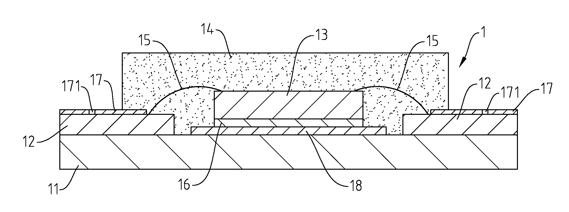
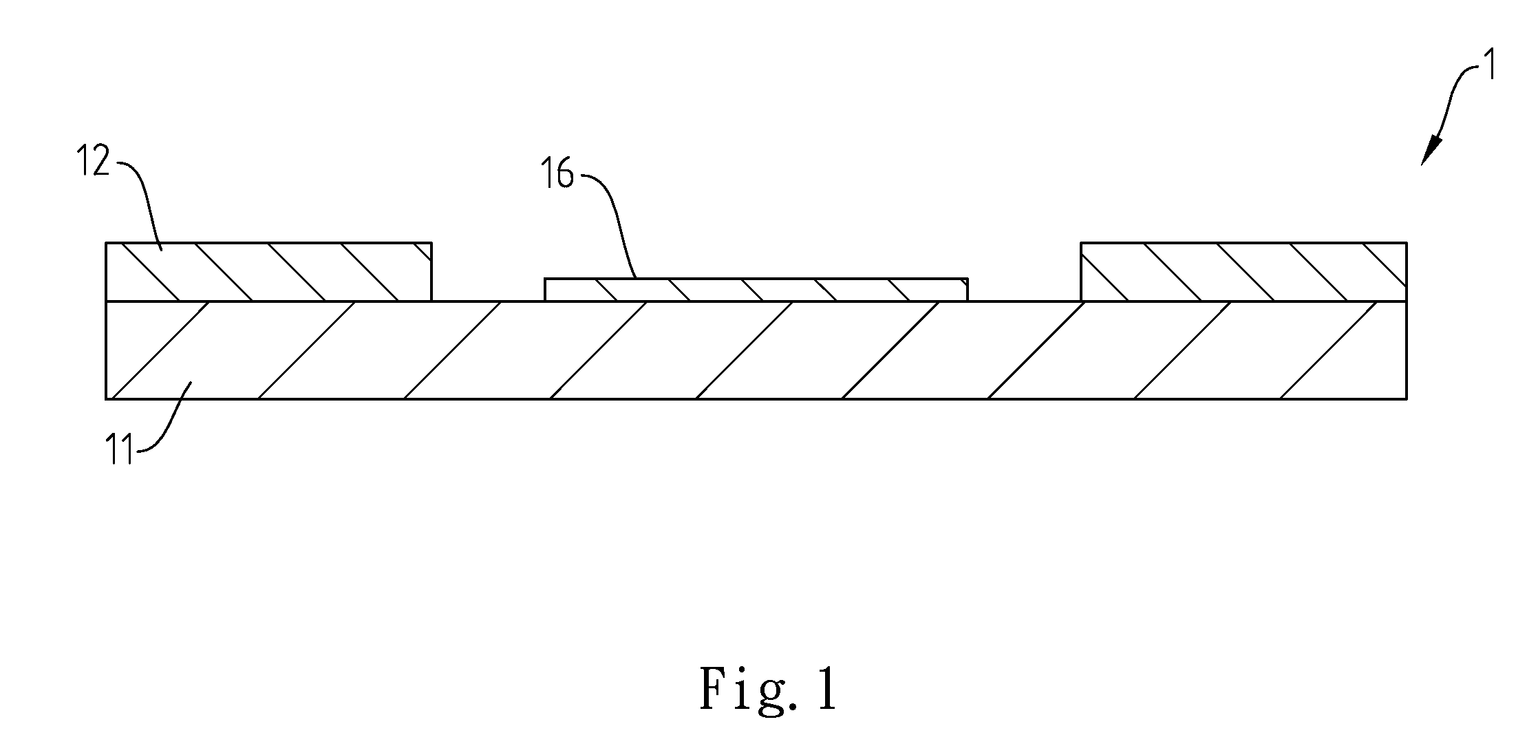
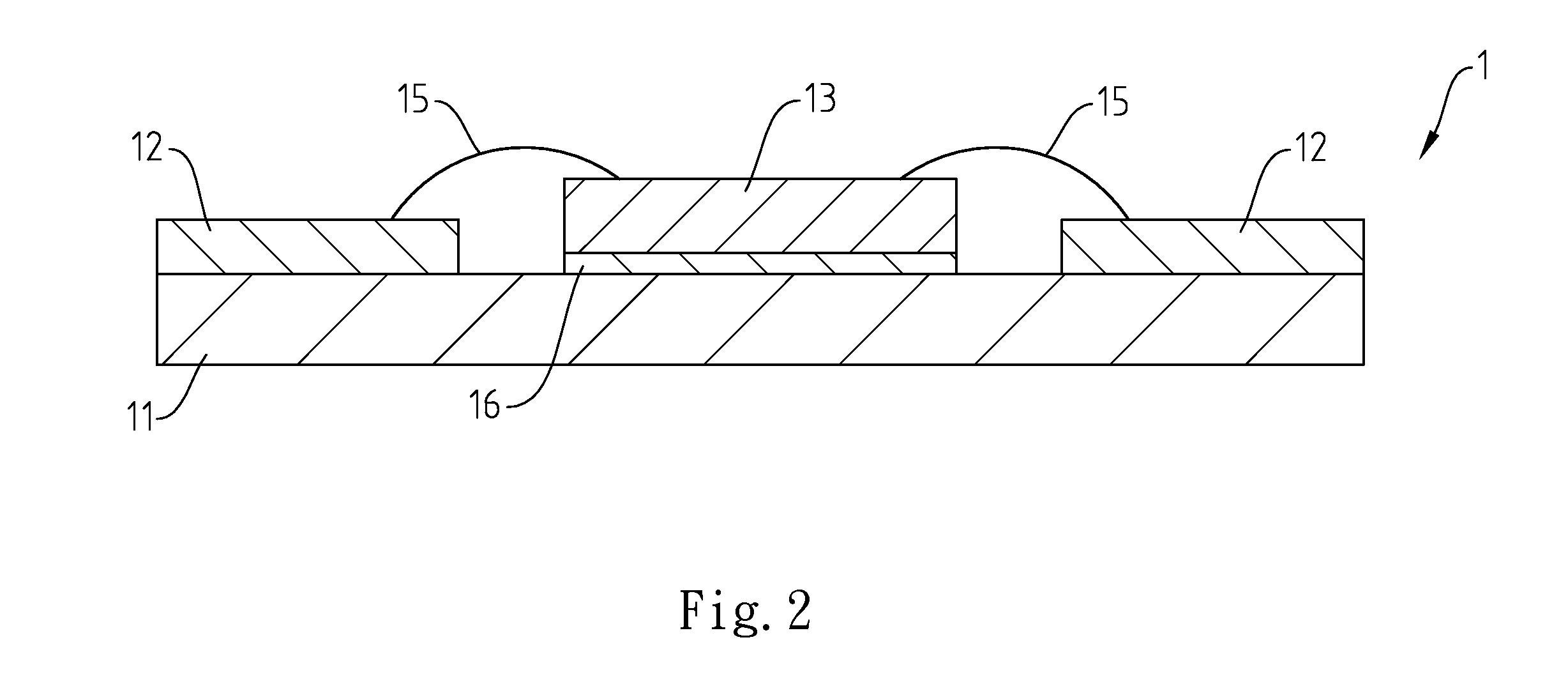
[0013]Referring to FIGS. 1˜3, a high-power LED package 1 in accordance with the present invention is made by: (1) preparing a thermal conductive substrate 11 from a material having a high heat transfer coefficient, for example, copper or aluminum; (2) forming a circuit layer 12 and a bonding layer 16 on the surface of the thermal conductive substrate 11, wherein the bonding layer 16 is formed by coating a solder material on the surface of the thermal conductive substrate 11; (3) mounting a LED chip 13 on the bonding layer 16; (4) bonding gold or aluminum lead wires of diameter about 10 μm to electrically connect the LED chip 13 to the circuit layer 12; and (5) applying a packaging material, for example, silver adhesive or epoxy resin to the thermal conductive substrate 11 to form a packaging layer 14 that covers the LED chip 13, the lead wires 15 and the connection areas between the lead wires 15 and the circuit layer 12 without reaching the periphery and bottom side of the thermal ...


PUM


Abstract

A high-power LED package includes a thermal conductive substrate, a circuit layer formed on the top wall of the thermal conductive substrate, a LED chip mounted on the top wall of the thermal conductive substrate, lead wires electrically connected between the LED chip and the circuit layer, and a packaging layer covering the LED chip, the lead wires and the connection areas between the lead wires and the circuit layer outside the bottom wall of the thermal conductive substrate for enabling waste heat to be directly transferred from the LED chip to the thermal conductive substrate and then rapidly dissipated into the outside open air by the thermal conductive substrate during operation of the LED chip.

Description

BACKGROUND OF THE INVENTION[0001]1. Field of the Invention[0002]The present invention relates to LED package technology and more particularly, to a high-power LED package, which has the characteristics of high performance, low power consumption, high reliability and long life span.[0003]2. Description of the Related Art[0004]The luminous efficiency of regular LEDs (light emitting diodes) is about 15˜20%, i.e., only about 15˜20% of inputted electric energy is converted into light energy, and the rest 80˜85% of inputted electric energy is converted into thermal energy. A relatively higher power LED generates a relatively greater amount of thermal energy during operation. If a LED package cannot effectively dissipate thermal energy, thermal energy will be cumulated inside the package, causing a rise in the contact point temperature. When the contact point temperature rises, the luminous efficiency of the LED package will drop, and the emission wavelength will become shortened, leading ...

Claims


Application Information

Patent Timeline
IPC IPC(8): H01L33/00
CPCH01L33/44H01L33/62H01L33/641H01L2224/73265H01L2224/48091H01L2924/00014
Inventor LIN, CHEN-WEILIAO, CHIA-YU
Owner H&T ELECTRONICS
Why Eureka
Try Eureka