Display apparatus, method of manufacturing display apparatus, and electronic apparatus

a technology of display apparatus and display device, which is applied in the direction of electrical apparatus, semiconductor devices, instruments, etc., can solve the problems of damage to uniformity of display device, and achieve the effect of reducing the capacitance value of parasitic capacitance, improving bootstrap gain, and improving bootstrap gain

Active Publication Date: 2011-10-06
JOLED INC
View PDF0 Cites 9 Cited by
  • Summary
  • Abstract
  • Description
  • Claims
  • Application Information

AI Technical Summary

Benefits of technology

[0015]The driving transistor has an LDD (Lightly Doped Drain) configuration in which the impurity regions with lower concentration than the source / drain regions, that is, LDD regions, are formed between the channel region and the first and second source / drain regions. When the LDD region and the gate electrode face each other in the LDD configuration, the parasitic capacitance is formed in the facing region. Therefore, the capacitance value of the parasitic capacitance is one of the parameters determining the bootstrap gain. Here, the LDD region located between the channel region and the first source / drain region is formed in the region other than the region facing the gate electrode. With such a configuration, the bootstrap gain can be improved since the capacitance value of the parasitic capacitance between the LDD region and the gate electrode, that is, between the gate and the source of the driving transistor is reduced.
[0016]According to the embodiments of the invention, the bootstrap gain can be improved by reducing the capacitance value of the parasitic capacitance between the gate and the source of the driving transistor. Therefore, the high-quality display image can be achieved without damage to the uniformity of a screen.

Problems solved by technology

As a consequence, the uniformity of a screen may be damaged.

Method used


Image

  • Display apparatus, method of manufacturing display apparatus, and electronic apparatus
  • Display apparatus, method of manufacturing display apparatus, and electronic apparatus
  • Display apparatus, method of manufacturing display apparatus, and electronic apparatus

Examples


embodiment

Configuration of Driving Transistor

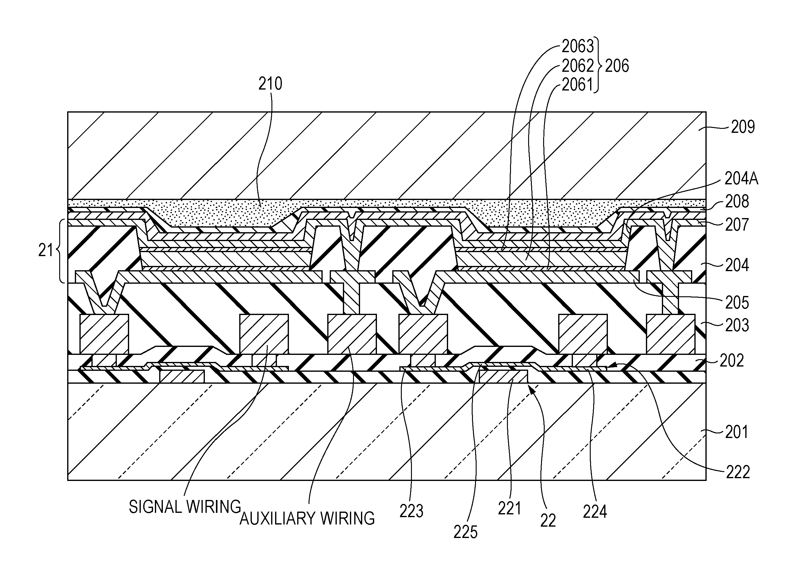
[0154]A specific embodiment of the driving transistor 22B will be described with reference to FIGS. 16A and 16B. FIGS. 16A and 16B are diagrams illustrating the configuration of the driving transistor 22B according to the embodiment. FIGS. 16A and 16B are a plan view and a sectional view illustrating the driving transistor 22B, respectively. The reference numerals are given to the same constituent elements as those of FIGS. 15A and 15B.

[0155]As shown in FIGS. 16A and 16B, the driving transistor 22B according to the embodiment is a bottom gate type transistor in which the gate electrode 221 is formed closer to the substrate than the channel region (channel formation region) 225. In addition, the driving transistor 22B according to the embodiment has the LDD configuration in which the impurity regions with lower concentration than that of the source / drain regions 223 and 224, that is, the LDD regions 226 and 227, are formed between the channel region...


PUM


Abstract

A display apparatus includes a plurality of pixels each including an electro-optic element, a writing transistor writing a video signal into the pixel, a holding capacitor holding the video signal written by the writing transistor, and a driving transistor driving the electro-optic element based on the video signal held in the holding capacitor. The driving transistor includes a channel region, a gate electrode disposed opposite to the channel region, a first source/drain region closer to a power source, a second source/drain region closer to the electro-optic element, and impurity regions disposed between the channel region and the first and second source/drain regions and having a lower concentration than that of the corresponding source/drain region. The impurity region disposed between the channel region and the first source/drain region is formed in a region other than a region facing the gate electrode.

Description

BACKGROUND OF THE INVENTION[0001]1. Field of the Invention[0002]The present invention relates to a display apparatus, a method of manufacturing the display apparatus, and an electronic apparatus, and more particularly, to a display apparatus in which pixels including an electro-optic element are arranged two-dimensionally in a matrix form, a method of manufacturing the display apparatus, and an electronic apparatus including the display apparatus.[0003]2. Description of the Related Art[0004]In recent years, in the field of display apparatuses displaying an image, flat type display apparatuses in which pixels (pixel circuits) are arranged in a matrix form have rapidly come into wide use. As one of the flat type display apparatuses, there is known a display apparatus in which a so-called current-driven-type electro-optic element, in which light emission luminance varies according to the value of current flowing in a device, is used as a light-emitting element. As the current-driven-ty...

Claims


Application Information

Patent Timeline
Patent Type & Authority Applications(United States)
IPC IPC(8): H01L27/15H01L33/16
CPCH01L27/1214H01L27/3262G09G2320/045G09G3/325G09G2300/0852H01L29/78624G09G2300/0819H10K59/1213
Inventor OMOTO, KEISUKE
Owner JOLED INC
Why Eureka
Try Eureka