
Method of making conductive Group lll Nitride single crystal substrate

Inactive Publication Date: 2011-10-06
HITACHI CABLE
View PDF9 Cites 1 Cited by
  • Summary
  • Abstract
  • Description
  • Claims
  • Application Information

AI Technical Summary

Benefits of technology

[0027]According to one embodiment of the invention, a method of making a conductive group III nitride single crystal substrate allows the SiH2Cl2 diluted with N2 or Ar to inhibit the reaction between the SiH2Cl2 and NH3 gas phases, and therefore the group III nitride single crystal to be grown fast and have the desired specific resistance. Also, the method allows the group III nitride s

Problems solved by technology

However, with respect to JP-A-2000-91234, JP-A-2006-193348 and JP-B-3985839, producing one GaN substrate requires the use of one hetero-substrate, and is therefore costly.
Also, with respect to JP-A-2006-273716 and JP-A-2003-17420, the GaN ingot to be sliced by a wafer slicer to produce the GaN single crystal substrates, requires a margin of a few mm to be cut, and in addition, a further few hundred μm of layers damaged by cutting to be ground at one surface of the GaN ingot, and is therefore costly.
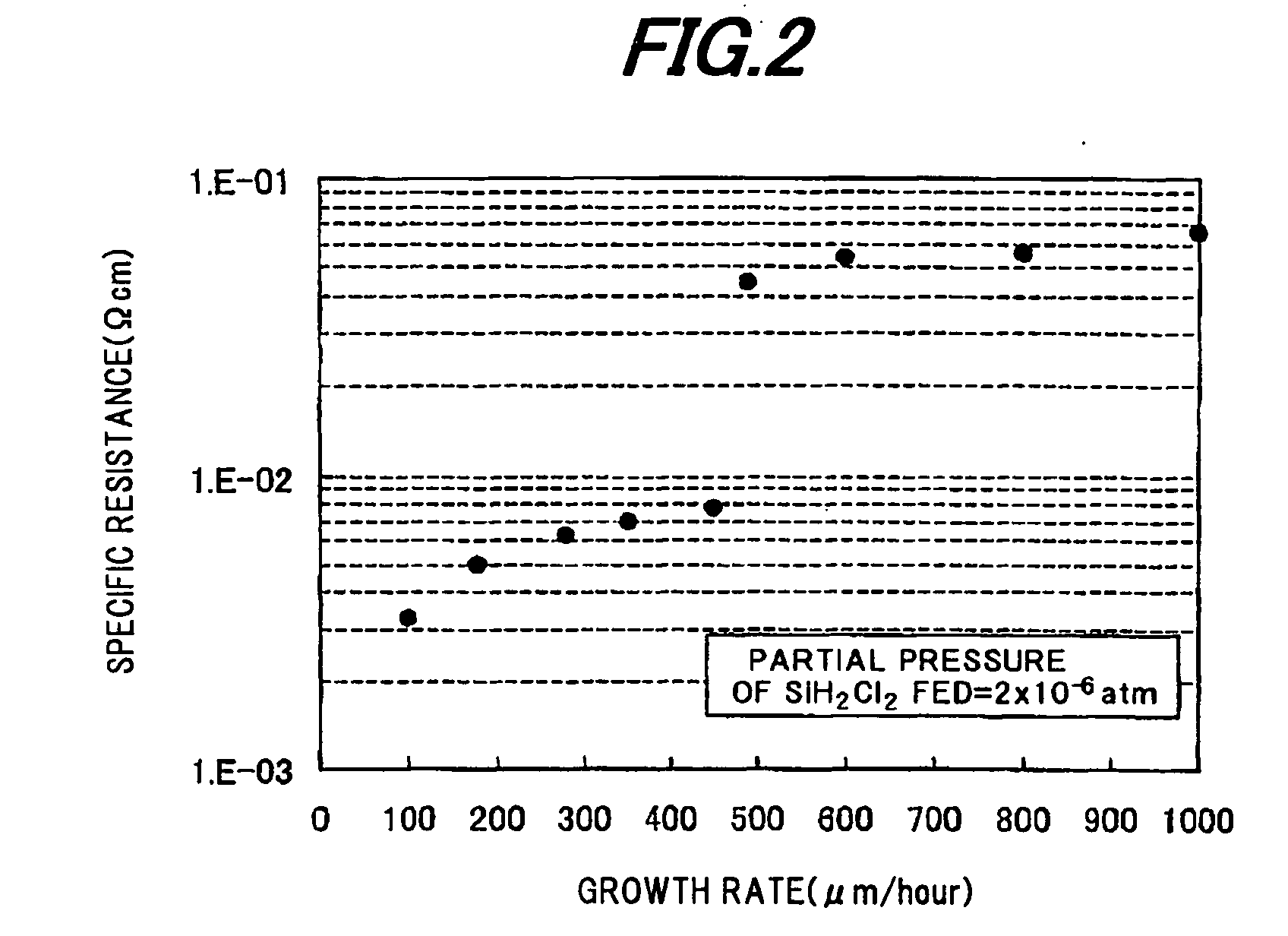
Further, with respect to Journal of Crystal Growth 311 (2009) 3011, JP-A-2000-91234, and JP-A-2003-17420, the GaN single crystal growth rate is on the order of one hundred μm / hour, and requires a long period of time for crystal growth to produce the GaN single crystal substrate, which is a few hundred μm thick, and which has a margin of a few mm to be cut, and producing the GaN single crystal substrate is therefore costly.

Method used


Image

  • Method of making conductive Group lll Nitride single crystal substrate
  • Method of making conductive Group lll Nitride single crystal substrate
  • Method of making conductive Group lll Nitride single crystal substrate

Examples


example 1

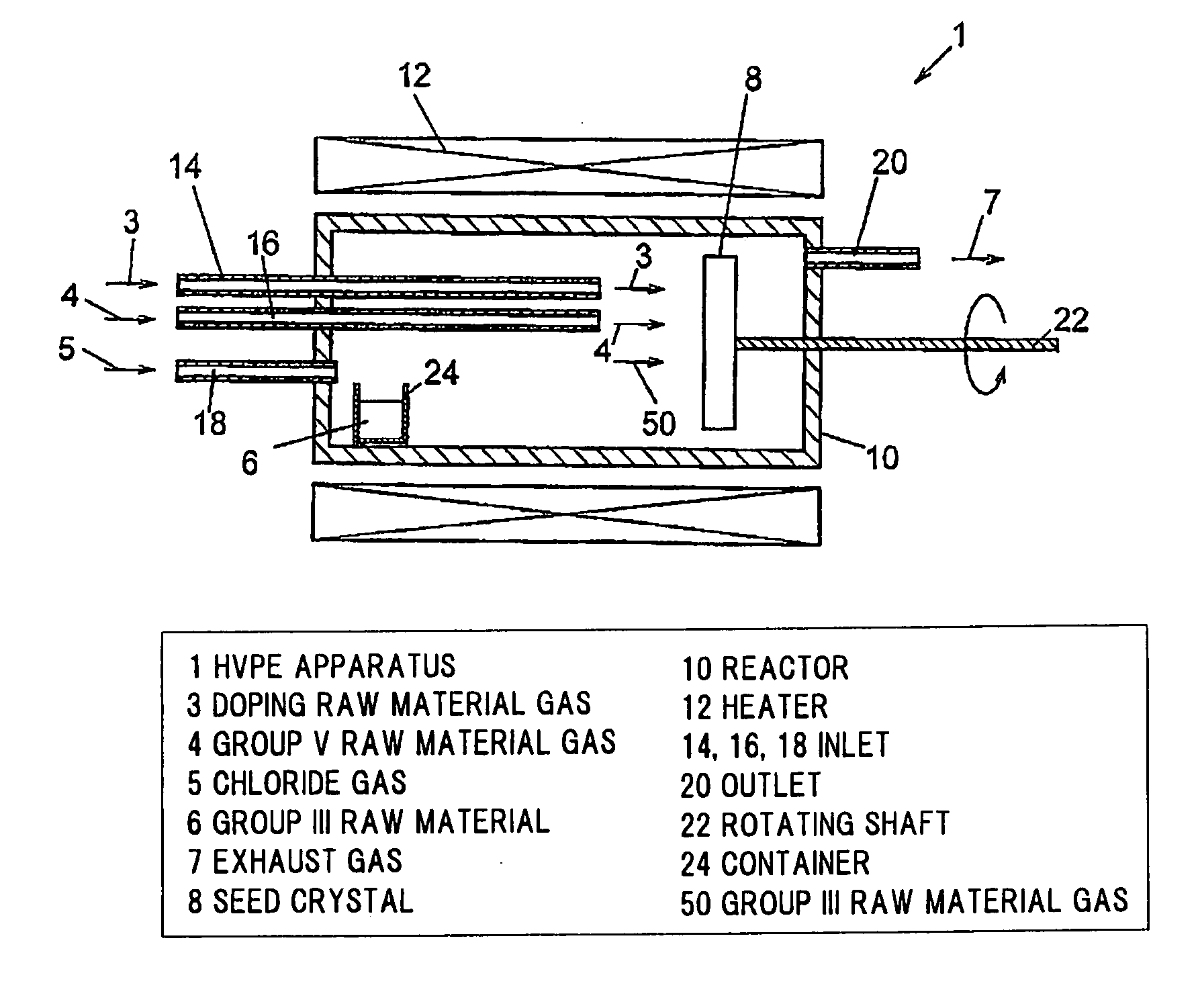
[0081]Now, described is Example 1 of the method of making the conductive group III nitride single crystal substrate. GaN single crystal ingots are fabricated by the HVPE as a group III nitride single crystal, using a 56 mm diameter GaN single crystal (0001) substrate as a seed crystal therefor. Herein, the group III nitride single crystals are AlxInyGa1-x-yN (0≦x≦1, 0≦y≦1, 0≦x+y≦1), of which the GaN single crystals are described as one example.

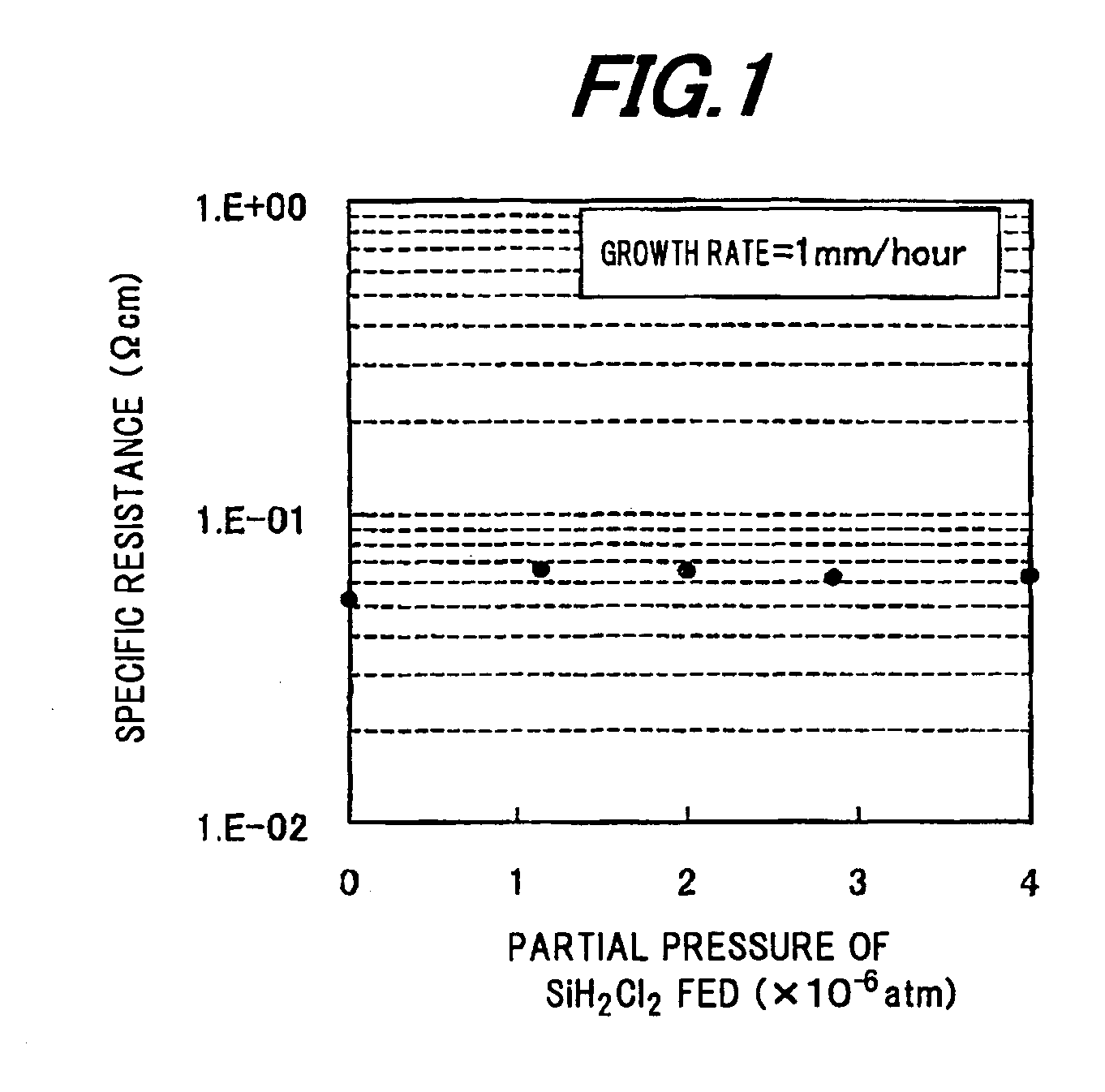
[0082]The partial pressure of each gas fed is as follows: the partial pressure of a GaCl gas fed for a group III raw material gas is 3×10⁻² atm, the partial pressure of an NH3 gas fed for a group V raw material gas is 20×10−2 atm, and the partial pressure of a H2 gas fed is 25×10−2 atm. Also used for a doping raw material gas is a SiH2Cl2 gas diluted with N2 to have a specified concentration of 300 ppm. The flow of the N2 diluted SiH2Cl2 gas fed is then adjusted to produce partial pressures of 0 atm, 0.14×10⁻⁶ atm, 0.29×10⁻⁶ atm, 0.57×10⁻⁶ atm...

example 2

[0087]Next, described is Example 2 of the method of making the conductive group III nitride single crystal substrate. GaN single crystal ingots are fabricated by the HVPE, using a 56 mm diameter GaN single crystal (0001) substrate as a seed crystal therefor.

[0088]The partial pressure of each gas fed is as follows: the partial pressure of a GaCl gas fed for a group III raw material gas is 6×10⁻² atm, the partial pressure of an NH3 gas fed for a group V raw material gas is 35×10−2 atm, and the partial pressure of a H2 gas fed is 25×10−2 atm. Also used for a doping raw material gas is a SiH2Cl2 gas diluted with N2 to have a specified concentration of 300 ppm. The flow of the N2 diluted SiH2Cl2 gas fed is then adjusted to produce partial pressures of 0 atm, 0.14×10⁻⁶ atm, 0.29×10⁻⁶ atm, 0.57×10⁻⁶ atm, 1.14×10⁻⁶ atm, and 2.86×10⁻⁶ atm.

[0089]Also, the growth area is in a range of 52 mm in diameter. The growth rate is 2 mm / hour. The thickness of the ingots is 3 mm.

[0090]Using the wafer sli...

example 3

[0093]Next, described is Example 3 of the method of making the conductive group III nitride single crystal substrate. GaN single crystal ingots are fabricated by the HVPE, using a 56 mm diameter GaN single crystal (0001) substrate as a seed crystal therefor.

[0094]The partial pressure of each gas fed is as follows: the partial pressure of a GaCl gas fed for a group III raw material gas is 2×10⁻² atm, the partial pressure of an NH3 gas fed for a group V raw material gas is 13×10−2 atm, and the partial pressure of a H2 gas fed is 25×10−2 atm. Also used for a doping raw material gas is a SiH2Cl2 gas diluted with N2 to have a specified concentration of 300 ppm. The flow of the N2 diluted SiH2Cl2 gas fed is then adjusted to produce partial pressures of 0 atm, 0.14×10⁻⁶ atm, 0.29×10⁻⁶ atm, 0.57×10⁻⁶ atm, 1.14×10⁻⁶ atm, and 2.86×10⁻⁶ atm.

[0095]Also, the growth area is in a range of 52 mm in diameter. The growth rate is 455 μm / hour. The thickness of the ingots is 3 mm.

[0096]Using the wafer s...


PUM

PropertyMeasurementUnit
Temperatureaaaaaaaaaa
Thicknessaaaaaaaaaa

Abstract

A method of making a conductive group III nitride single crystal substrate includes feeding to a seed crystal a group III raw material gas, a group V raw material gas, and a doping raw material gas diluted with N2 or Ar to have a predetermined concentration, growing a group III nitride single crystal on the seed crystal at a growth rate of greater than 450 μm / hour and not greater than 2 mm / hour, and doping the group III nitride single crystal with an impurity contained in the doping raw material gas. The doping raw material gas is diluted to be inhibited from reacting with the group V raw material gas so as to allow the group III nitride single crystal to have a specific resistance of not less than 1×10⁻³ Ωcm and not more than 1×10⁻² Ωcm.

Description

[0001]The present application is based on Japanese patent application No. 2010-084816 filed on Apr. 1, 2010, the entire contents of which are incorporated herein by reference.BACKGROUND OF THE INVENTION[0002]1. Field of the Invention[0003]This invention relates to a method of making a conductive group III nitride single crystal substrate.[0004]2. Description of the Related Art[0005]En recent years, most of GaN single crystal substrates have been produced by using halide vapor phase epitaxy (HVPE). The known method to produce a conductive GaN single crystal substrate by the HVPE is to feed as a doping gas SiHxCl4-x (x=1 to 3), or an O2, H2O, H2S, SiCl4, GeCl4, Se2Cl2, Te2Cl2 or the like, to dope the GaN single crystal grown on a surface of a hetero-substrate (Al2O3, SiC or the like) (see below listed JP-A-2000-91234, Journal of Crystal Growth 311 (2009) 3011, Kenji Fujito, Shuichi Kubo, Hirobumi Nagaoka, Tae Mochizuki, Hideo Namita, and Satoru Nagao, and JP-A-2006-193348).[0006]Also,...

Claims


Application Information

Patent Timeline
IPC IPC(8): B24B7/22H01L21/322
CPCB24B7/228B24B7/17
Inventor YOSHIDA, TAKEHIRO
Owner HITACHI CABLE
Learn More