Detection element for detecting an electromagnetic wave

Inactive Publication Date: 2011-10-13
CANON KK
View PDF16 Cites 20 Cited by
  • Summary
  • Abstract
  • Description
  • Claims
  • Application Information

AI Technical Summary

Benefits of technology

[0008]According to the electromagnetic wave detection element of the present invention, the antenna is formed across multiple surfaces located at different level positions along the incident direction of the electrom

Problems solved by technology

Cooling is not always required, but a response is relatively slow because heat exchange is used.
The response is relatively fast, but cooling is required because a thermal energy of a room temperature in such a frequency range cannot be ignored.
This is because, in order to support the freque

Method used


Image

  • Detection element for detecting an electromagnetic wave
  • Detection element for detecting an electromagnetic wave
  • Detection element for detecting an electromagnetic wave

Examples


first embodiment

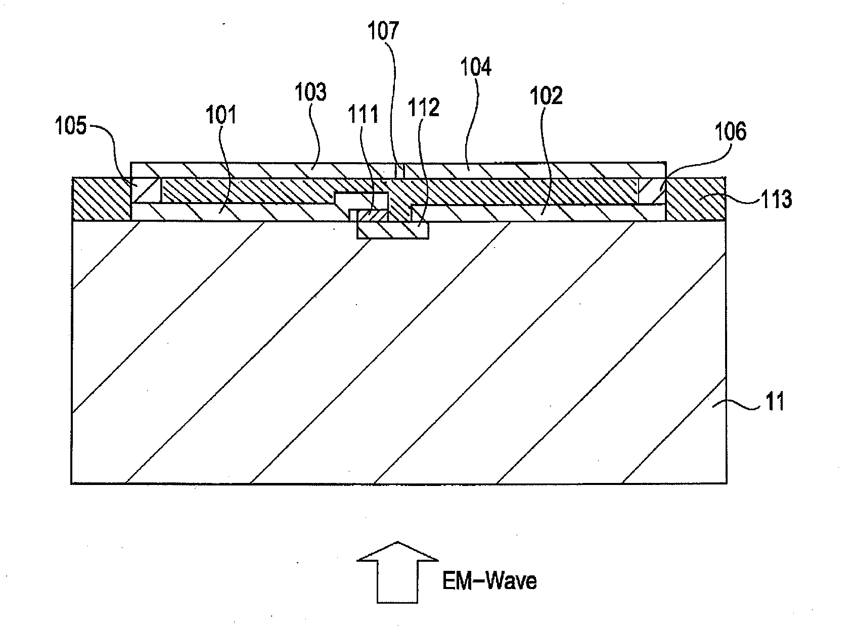
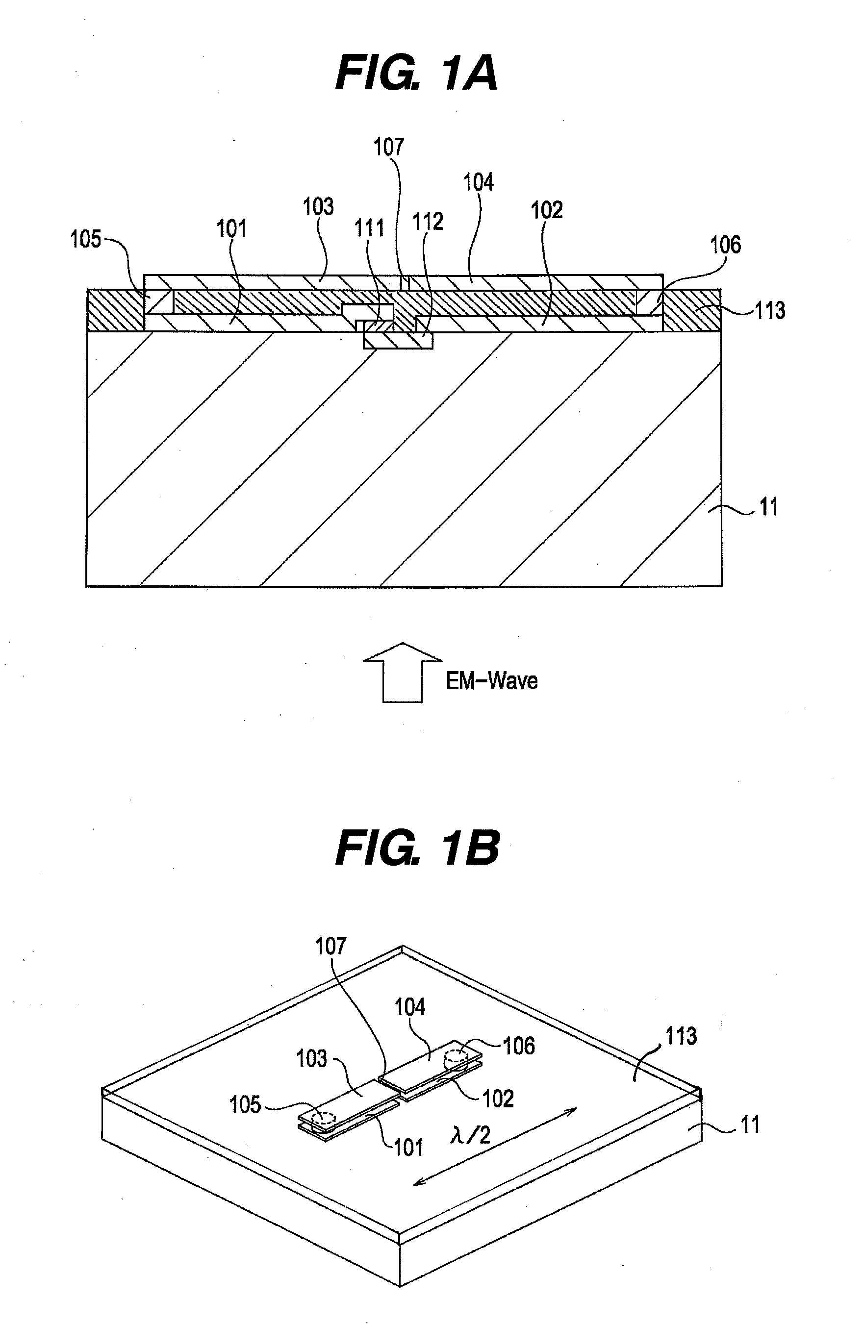
[0029]A detection element according to a first embodiment of the present invention is described with reference to FIGS. 1A and 1B. FIG. 1A is a cross-sectional view illustrating the detection element according to this embodiment, and FIG. 1B is a perspective view thereof.

[0030]The detection element according to this embodiment includes four conductive elements constituting an antenna, and two vias that are connecting members. Each of a divided first conductive element 101 and a divided second conductive element 102 is formed of a stripe metal film whose length is ¼ of a wavelength of the electromagnetic wave (λ / 4). The elements 101 and 102 constitute a λ / 2 dipole antenna, and a length direction thereof is a resonant direction of the electromagnetic wave. λ is a wavelength of the electromagnetic wave to be detected, which is not in a vacuum but is an effective wavelength multiplied by a wavelength compression ratio depending on a substrate 11. The elements 101 and 102 come into conta...

second embodiment

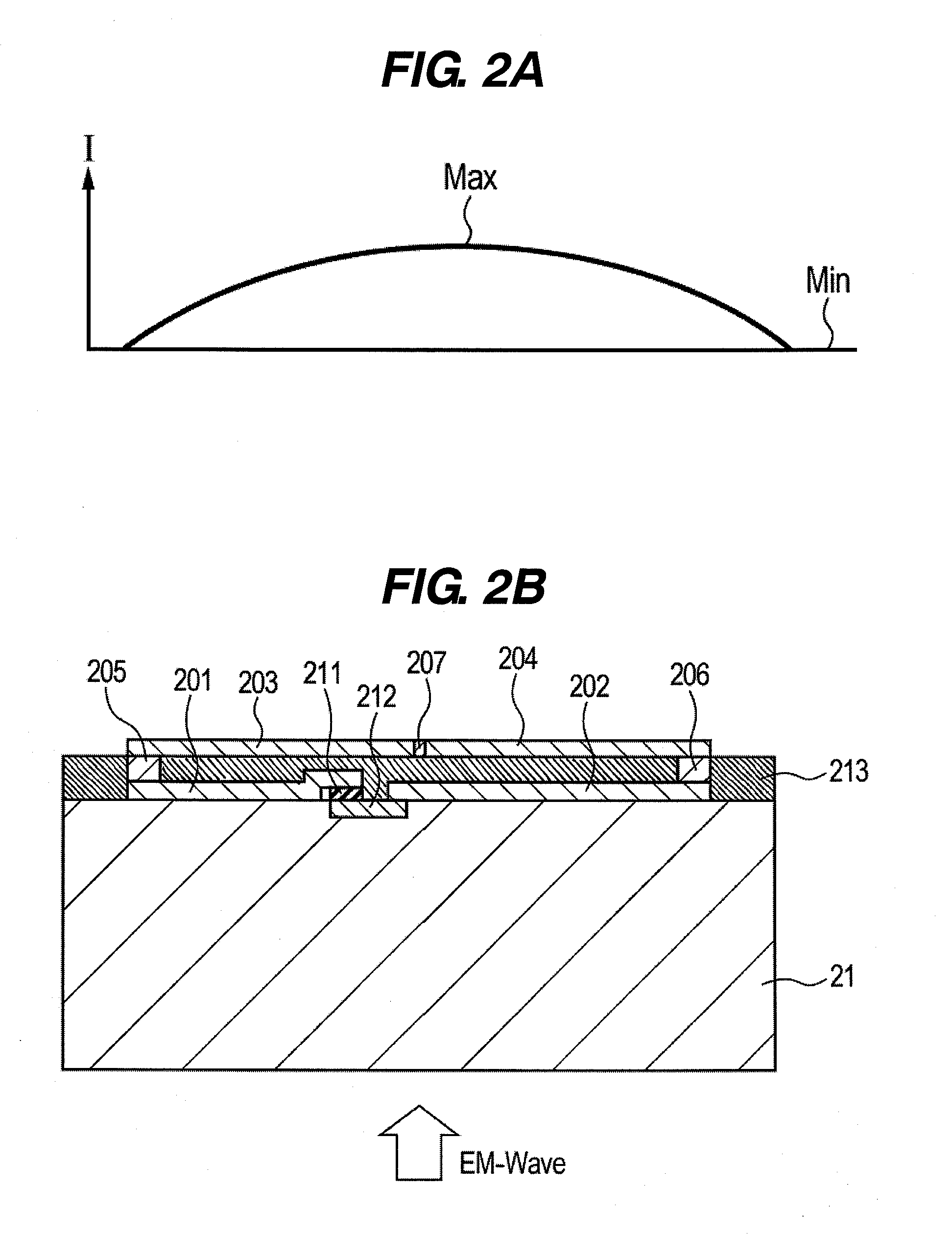
[0037]A detection element according to a second embodiment is described with reference to FIGS. 2A and 2B. In this embodiment, as illustrated in FIG. 2B, lengths of elements 201 and 202 and positions of semiconductors 211 and 212 are different from those in the first embodiment. The others are identical with those in the first embodiment. That is, elements 203 and 204, vias 205 and 206, a DC cut 207, and a dielectric material 213 are identical with those in the first embodiment. A sum of the lengths of the elements 201 and 202 is λ / 2, and the elements 201 and 202 are still λ / 2 dipole antenna. This embodiment is a modified example of the first embodiment in which positions of the schottky barrier diodes 201, 211, 212, and 202 are offset for increasing the input impedance of the antenna.

[0038]As shown in FIG. 2A, a current distribution I of the detected electromagnetic wave on the elements 201 and 202, and the elements 203 and 204 is minimum at positions corresponding to edges of the ...

third embodiment

[0039]A detection element according to a third embodiment is described with reference to FIG. 3. The detection element according to this embodiment includes four elements and two vias which constitute an antenna, and a metal film element 308 which is an additional fifth conductive element. In this embodiment, elements 301, 302, 303, and 304, vias 305 and 306, a DC cut 307, semiconductors 311 and 312, and a dielectric material 313 are identical with those in the first embodiment. The additional element 308 is located on a rear surface of a substrate 31 which is a surface opposite to the surface of the substrate on which the antenna is disposed, and a length thereof is set to be slightly longer than λ / 2. This embodiment shows an example in which the directivity of the antenna in the first embodiment is changed to a surface direction of the substrate 31 (upward in FIG. 3).

[0040]The element 308 slightly longer than λ / 2 derives from a technique called “reflector” that has been known by Y...


PUM


Abstract

A detection element for detecting an electromagnetic wave includes: a substrate; a schottky barrier diode disposed on the substrate; and an antenna disposed on the substrate, wherein the antenna includes a first conductive element and a second conductive element which are divided, a third conductive element and a fourth conductive element which are divided, a first connecting member that electrically connects the first conductive element and the third conductive element, and a second connecting member that electrically connects the second conductive element and the fourth conductive element, wherein the first conductive element and the second conductive element, and the third conductive element and the fourth conductive element are formed on multiple surfaces of the substrate, which are spaced apart from each other along an incident direction of the electromagnetic wave, respectively, and wherein the schottky barrier diode is electrically connected between the first conductive element and the second conductive element.

Description

BACKGROUND OF THE INVENTION[0001]1. Field of the Invention[0002]The present invention relates to an electromagnetic wave detection element using a rectifier element, and more particularly, to an electromagnetic wave detection element in a frequency band within a frequency range from a millimeter waveband to a terahertz band (a range of from 30 GHz to 30 THz, hereinafter used in the same sense), and a device using the electromagnetic wave detection element.[0003]2. Description of the Related Art[0004]As the electromagnetic wave detection element from a millimeter waveband to a terahertz band, a thermal detection element and a quantum detection element have been known up to now. The thermal detection element includes a microbolometer (a-Si, VOx, etc.), a pyroelectric element (LiTaO3, TGS, etc.), a Golay cell, and the like. Such a thermal detection element converts a physical change caused by an energy of an electromagnetic wave into heat, and converts a temperature change into a therm...

Claims


Application Information

Patent Timeline
IPC IPC(8): G01R27/04
CPCH01Q9/265H01Q1/248
Inventor SEKIGUCHI, RYOTA
Owner CANON KK
Why Eureka
Try Eureka