Integrated display and photovoltaic element

a technology of photovoltaic elements and integrated displays, which is applied in the manufacture of electric discharge tubes/lamps, basic electric elements, instruments, etc., can solve the problems of reducing contrast, operating at voltages too high to be compatible with active matrix driving circuits, and enhancing light trapping and absorption of specific wavelengths, so as to improve the brightness of the display. , the effect of generating electrical power efficiently

Inactive Publication Date: 2011-10-13
SHARP KK
View PDF4 Cites 51 Cited by
  • Summary
  • Abstract
  • Description
  • Claims
  • Application Information

AI Technical Summary

Benefits of technology

[0054]Alternatively, the additional reflecting layer 36 may reflect all or part of the visible spectrum while transmitting infra-red light, while the PV element is optimized to absorb infra-red light. For example, the PV element may be a cadmium telluride photovoltaic element. Again, this has the advantage of improving the brightness of the display while allowing the PV element to generate electrical power efficiently.
[0055]Alternatively, the additional layer 36 may comprise a periodic array of conducting nanostructures that support surface plasmons. The array of nanostructures may be designed to enhance light trapping and absorption of specific wavelengths by the PV element as described by Pala et al., Adv. Mater., 21, (2009), 3504-3509. In this way the spectrum and / or intensity of the reflected light may be controlled in order to improve the brightness of the display or show colour images, as described above, while simultaneously substantially preserving or increasing the efficiency of the PV element.
[0056]Alternatively, the additional layer 36 comprising a period array of conducting nanostructures may be combined with layer 16 to provide the dual function of enhanced light absorption by, and carrier extraction from the PV element.
[0057]Alternatively, the additional layer 36 may not be reflective in the conventional sense, but be composed of a dielectric material with a relatively low (n<1.35) refractive index. The purpose of inserting such a layer is that when the liquid crystal is in the non-scattering state, the incident light passes directly into the solar cell (aside from reflection losses), but in the scattering state, a significant fraction of the scattered light radiating from the PNLC layer is reflected away from the solar cell and back to the viewer, via the well-known process of total-internal-reflection. Some light will always pass into the solar cell, as before, but a greater fraction is reflected back to the viewer, resulting in a brighter display, without compromising the quality of the dark state by introducing reflectors into layer 36. Here, the low index layer occupies the position of layer 36 in FIG. 9. However, an alternative arrangement is for the low index layer 36 and the insulating layer 31 to be situated above the lower electrode for the PNLC layer. This has the disadvantage that some of the driving voltage for the PNLC layer will be dropped across inactive dielectric layers, but the advantage that the via hole necessary to connect the pixel electrode to the TFT circuitry is much shorter.
[0058]The PV element can be sub-divided into smaller PV elements that are cascaded in series by monolithic contacts where the pitch of the monolithic contacts is an integer multiple of the pixel pitch. This as the advantages of 1) avoiding moiré fringes or other observable patterns on the display; 2) decreasing output current of the smaller PV elements thereby reducing series resistance losses; 3) increasing the output voltage of the cascade to improve compatibility with external circuits to which they are connected.
[0059]Each smaller PV element in a single cascade can be further sub-divided to form two or more cascades. Each cascade can be connected in parallel to the other cascades. This has the advantage of reducing the impact of partial shading of the display on the efficiency of the PV layer.

Problems solved by technology

Photovoltaic power generation devices also are used in some of these devices and must occupy large areas to generate significant amounts of power.
However the reflecting layer has the disadvantage of increasing the brightness of the dark state, and therefore reducing the contrast.
However these devices normally operate at voltages too high to be compatible with active-matrix (TFT) driving circuits.
On the other hand, if the photon energy is greater than the band gap, the excess energy will be lost in the form of heat.
As a result of these factors thin film solar cells typically only make efficient use of a region of the solar spectrum between a lower limit set by the band gap of the light absorbing layer and an upper limit set by any additional windows layers in the cell.
This method has two disadvantages: since separate substrates are used for the display and the PV, the weight and thickness of the combined device are large; and when an active matrix is used in the display, the electronics of the active matrix absorb some light before it reaches the PV, reducing the PV efficiency.
Again, the efficiency of the PV is reduced in this arrangement because it occupies only part of the available area.
The energy of light striking parts of the display area not covered by PV is lost.
Again, the disadvantage is that because the PV occupies only a small part of the area, it can gather only a small part of the light energy falling on the device.

Method used


Image

  • Integrated display and photovoltaic element
  • Integrated display and photovoltaic element
  • Integrated display and photovoltaic element

Examples


first embodiment

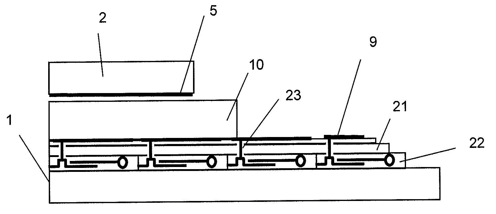
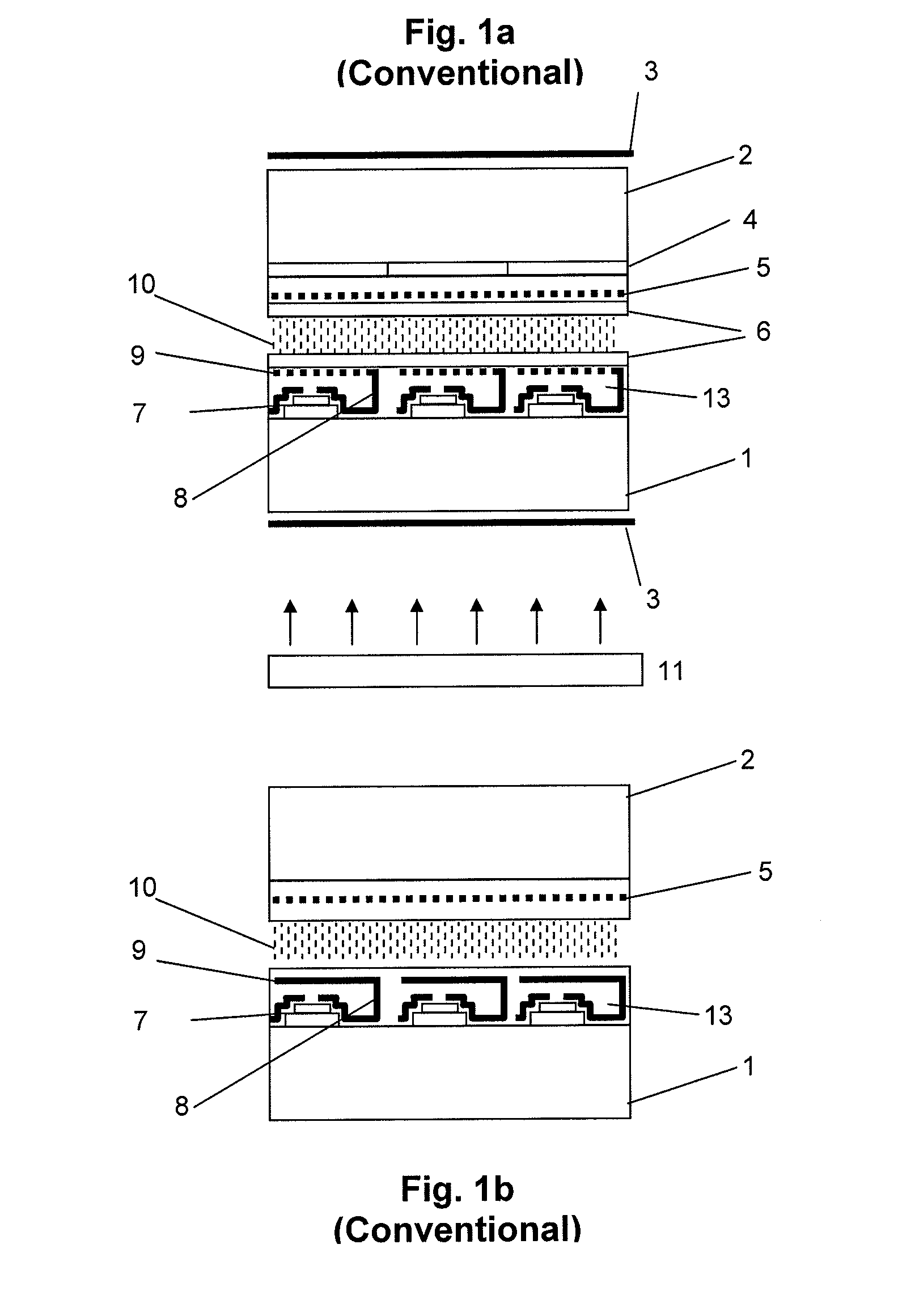
[0100]In a first embodiment of the invention, shown in FIG. 4, the display device is a polymer network liquid crystal display (PN-LCD), as described by Y. Asaoka et al in SID Symposium Proceedings 2009 paper 29.1 and in the other publications referred to above. The driving electronics include a memory device in every pixel which greatly reduces power consumption of the display. This memory device is also described in the paper by Asaoka.

[0101]Voltage is applied to the PN-LCD layer 10 by a transparent ITO common electrode 5 on the top substrate 2, and by ITO pixel electrodes 9 on the lower substrate 1. Below the pixel electrodes is a thin-film amorphous silicon PV element 21, which has the same structure as in FIG. 2(a). Each pixel electrode is connected to the driving electronics 22 for that pixel (which include a memory element as described above) by a conducting path or via connection 23 through the PV element 21.

[0102]FIG. 5 shows a schematic view of the structure of two adjacent...

second embodiment

[0111]A second embodiment of the invention is the same as the first embodiment except that the liquid crystal layer 10 is a reverse-mode polymer network LCD, as described, for example, in U.S. Pat. No. 5,188,760 (Hikmet; Philips) mentioned above.

third embodiment

[0112]A third embodiment of the invention is the same as the first embodiment except that the liquid crystal layer 10 is replaced with either an electrowetting or an in-plane electrophoretic layer.


PUM

PropertyMeasurementUnit
refractive indexaaaaaaaaaa
thicknessaaaaaaaaaa
wavelengthsaaaaaaaaaa

Abstract

A display device includes a first layer having an optically active display portion, a second layer including a photovoltaic element, and a third layer including electronics operatively coupled to the first layer, wherein the electronics are configured to drive the optically active display portion. Further, the second layer is arranged between the first and third layers.

Description

TECHNICAL FIELD[0001]The present invention relates generally to display devices and, more particularly, to a device and method that combines a display element and a photovoltaic element so that they occupy the same area and both operate as efficiently as possible.BACKGROUND ART[0002]Displays such as liquid crystal displays (LCDs) and organic LED displays (OLEDs) occupy a significant part of the surface of many electronic devices such as mobile telephones, televisions and monitors. Photovoltaic power generation devices also are used in some of these devices and must occupy large areas to generate significant amounts of power.Liquid Crystal Displays[0003]FIGS. 1a and 1b show schematic diagrams of typical active-matrix liquid crystal displays. FIG. 1a is a colour transmissive display, and FIG. 1b is a monochrome reflective display.[0004]In each case, the display is constructed on two substrates 1 and 2. These are typically glass but may also be polymer. The liquid crystal layer 10 is a...

Claims


Application Information

Patent Timeline
Patent Type & Authority Applications(United States)
IPC IPC(8): G02F1/1335G02F1/1333H01J9/24
CPCG02F1/13306G02F2001/13324G02F1/136227G02F1/13324
Inventor EVANS, ALLANDAY, STEPHENSHAH, SUNAYZEBEDEE, PATRICKPARRY-JONES, LESLEYNICHOLAS, GARETH
Owner SHARP KK
Why Eureka
Try Eureka