

Semiconductor device and method for manufacturinmg the same
a semiconductor memory device and semiconductor technology, applied in the direction of semiconductor memory devices, basic electric elements, electrical appliances, etc., can solve the problems of increasing power consumption, degrading the operation stability of the semiconductor memory device, and the device cannot output data stored in a unit cell to the outsid
- Summary
- Abstract
- Description
- Claims
- Application Information
AI Technical Summary
Benefits of technology
Problems solved by technology
Method used
Image

Examples
Embodiment Construction
[0040]The present invention will be described in detail with reference to the attached drawings.
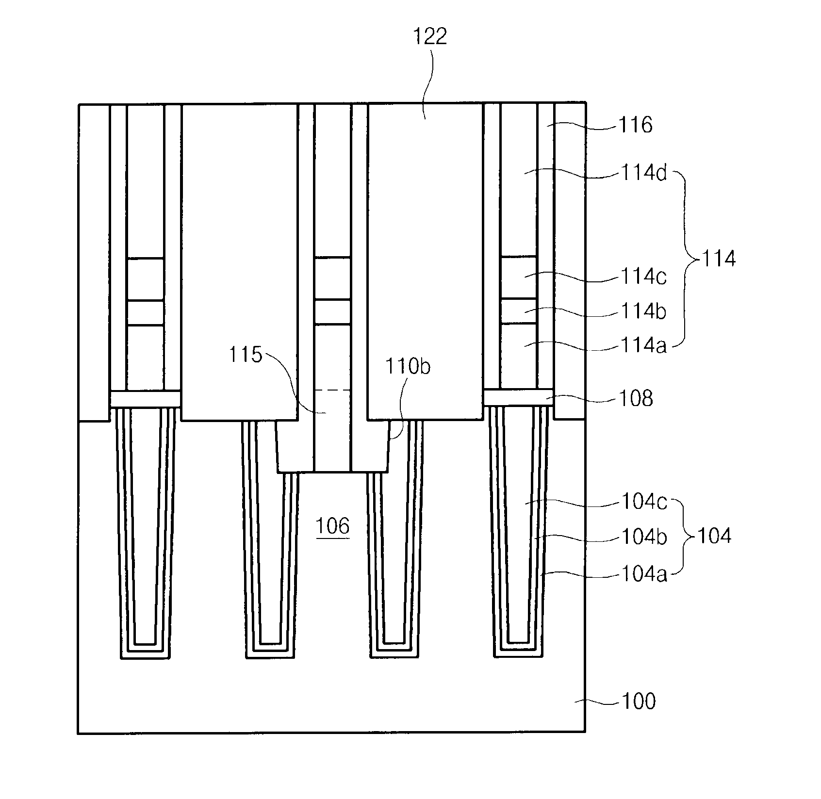
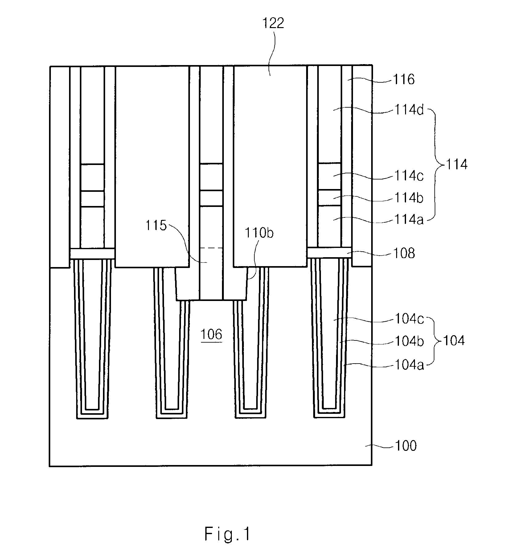
[0041]FIG. 1 is a cross-sectional diagram illustrating a semiconductor device according to an embodiment of the present invention.
[0042]Referring to FIG. 1, the semiconductor device comprises a bit line 114 formed on a semiconductor substrate 100 including an active region 106 defined as a device isolation film 104, a bit line contact plug 115 disposed in the lower portion of the bit line 114 to have the same width as the bit line 114, a spacer insulating film 116 formed in sidewalls of the bit line contact plug 115 and the bit line 114, and a storage node contact plug 122 disposed between the bit lines 114 and insulated from the bit line 114 by the spacer insulating film 116.
[0043]The bit line contact plug 115 connected to the active region 106 in a bit line contact hole obtained by etching a given thickness of the semiconductor substrate 100 has a smaller width than that of the bit line...
PUM
 Abstract
Description
Claims
Application Information