Cadmium sulfide layers for use in cadmium telluride based thin film photovoltaic devices and methods of their manufacture

a technology of cadmium telluride and thin film, applied in the direction of final product manufacturing, sustainable manufacturing/processing, vacuum evaporation coating, etc., can solve the problem of radiation passing through the cadmium sulfide layer

Inactive Publication Date: 2011-11-03
FIRST SOLAR INC (US)
View PDF2 Cites 11 Cited by
  • Summary
  • Abstract
  • Description
  • Claims
  • Application Information

AI Technical Summary

Problems solved by technology

However, the optical bandgap of cadmium sulfide of about 2.42 eV limits the amount of radiation that can pass through the cadmium sulfide layer in the blue through ultraviolet.

Method used


Image

  • Cadmium sulfide layers for use in cadmium telluride based thin film photovoltaic devices and methods of their manufacture
  • Cadmium sulfide layers for use in cadmium telluride based thin film photovoltaic devices and methods of their manufacture
  • Cadmium sulfide layers for use in cadmium telluride based thin film photovoltaic devices and methods of their manufacture

Examples


Embodiment Construction

[0016]Reference now will be made in detail to embodiments of the invention, one or more examples of which are illustrated in the drawings. Each example is provided by way of explanation of the invention, not limitation of the invention. In fact, it will be apparent to those skilled in the art that various modifications and variations can be made in the present invention without departing from the scope or spirit of the invention. For instance, features illustrated or described as part of one embodiment can be used with another embodiment to yield a still further embodiment. Thus, it is intended that the present invention covers such modifications and variations as come within the scope of the appended claims and their equivalents.

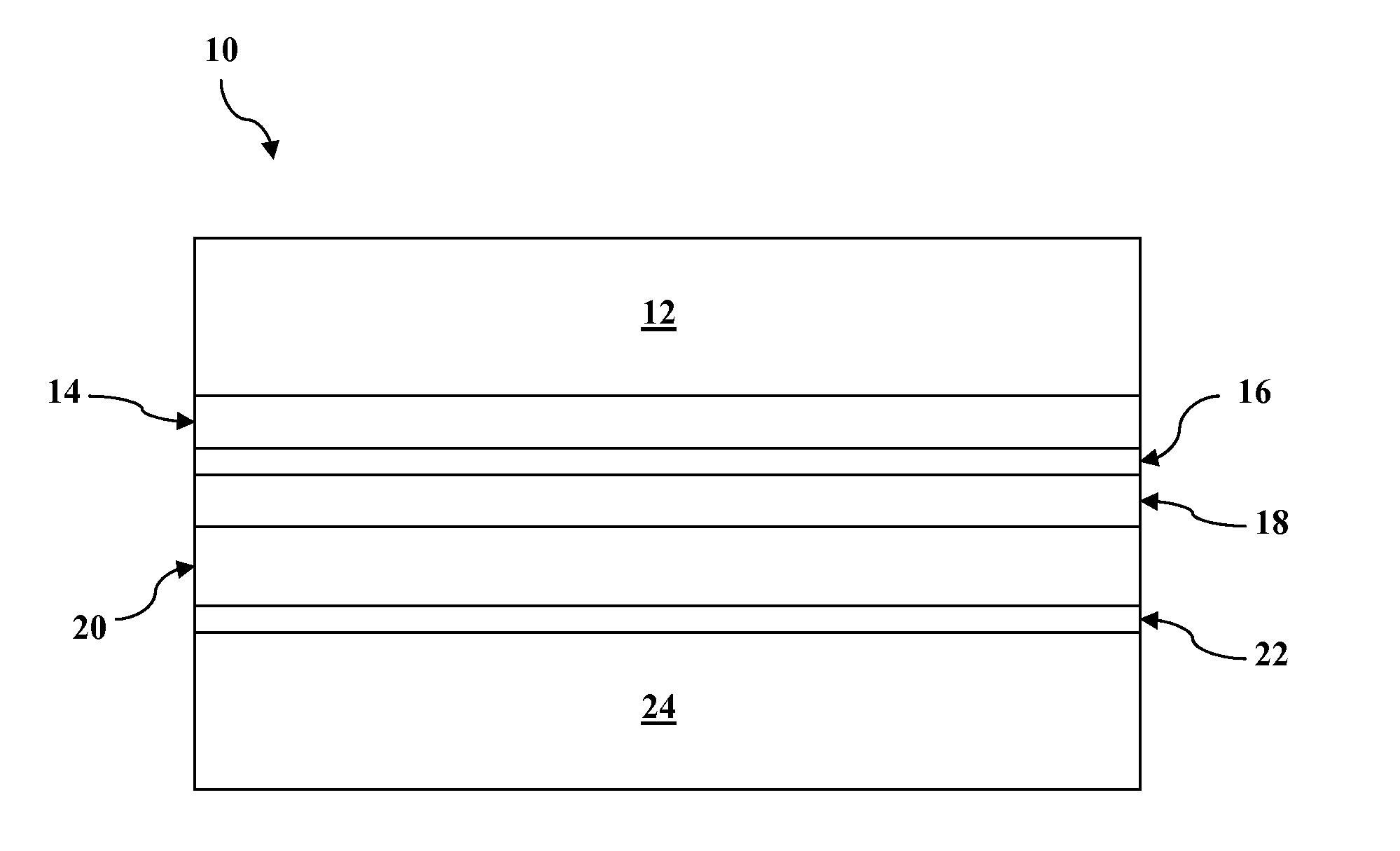
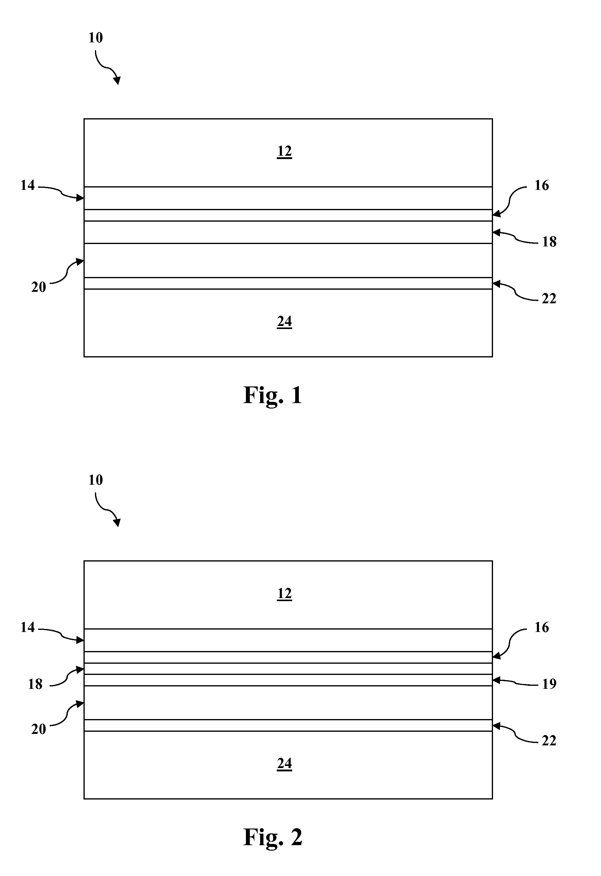
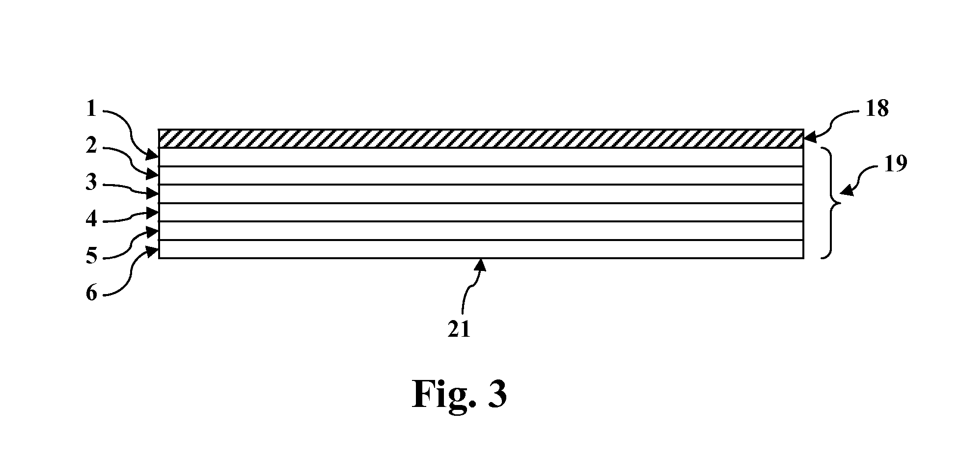
[0017]In the present disclosure, when a layer is being described as “on” or “over” another layer or substrate, it is to be understood that the layers can either be directly contacting each other or have another layer or feature between the layers. Thus, the...


PUM

PropertyMeasurementUnit
energy bandgapaaaaaaaaaa
thicknessaaaaaaaaaa
pressureaaaaaaaaaa

Abstract

Methods are generally provided for forming a cadmium sulfide layer on a substrate. In one particular embodiment, the method can include sputtering a cadmium sulfide layer on a substrate in a sputtering atmosphere comprising an inorganic fluorine source gas. Methods are also generally provided for manufacturing a cadmium telluride based thin film photovoltaic device.
Cadmium telluride based thin film photovoltaic devices are also generally provided. The device can include a substrate; a transparent conductive oxide layer on the substrate; a cadmium sulfide layer on the transparent conductive oxide layer; and, a cadmium telluride layer on the cadmium sulfide layer. The cadmium sulfide layer includes fluorine.

Description

FIELD OF THE INVENTION[0001]The subject matter disclosed herein relates generally to cadmium sulfide thin film layers and their methods of deposition. More particularly, the subject matter disclosed herein relates to cadmium sulfide layers for use in cadmium telluride thin film photovoltaic devices and their methods of manufacture.BACKGROUND OF THE INVENTION[0002]Thin film photovoltaic (PV) modules (also referred to as “solar panels”) based on cadmium telluride (CdTe) paired with cadmium sulfide (CdS) as the photo-reactive components are gaining wide acceptance and interest in the industry. CdTe is a semiconductor material having characteristics particularly suited for conversion of solar energy to electricity. For example, CdTe has an energy bandgap of about 1.45 eV, which enables it to convert more energy from the solar spectrum as compared to lower bandgap semiconductor materials historically used in solar cell applications (e.g., about 1.1 eV for silicon). Also, CdTe converts ra...

Claims


Application Information

Patent Timeline
Patent Type & Authority Applications(United States)
IPC IPC(8): H01L31/0296H01L31/18C23C14/34
CPCC23C14/0629C23C14/34H01L31/0296Y02E10/543H01L31/073H01L31/1828H01L31/1836H01L31/02963Y02P70/50
Inventor GOSSMAN, ROBERT DWAYNEPAVOL, MARK JEFFREY
Owner FIRST SOLAR INC (US)
Why Eureka
Try Eureka