High-pixel infrared focal plane array detector and preparation method thereof

A high pixel and detector technology, applied in the field of infrared focal plane detection, can solve the problems of epitaxial wafer surface unevenness, etc., and achieve the effects of avoiding cracks or damage, uniform force, and avoiding the introduction of stress

Active Publication Date: 2016-08-17
WUHAN GAOXIN TECH
View PDF3 Cites 8 Cited by
  • Summary
  • Abstract
  • Description
  • Claims
  • Application Information

AI Technical Summary

Problems solved by technology

[0004] In view of this, it is necessary to address the above-mentioned problems, provide a high-pixel infrared focal plane detector and its preparation method, solve the pro...

Method used


Image

  • High-pixel infrared focal plane array detector and preparation method thereof
  • High-pixel infrared focal plane array detector and preparation method thereof
  • High-pixel infrared focal plane array detector and preparation method thereof

Examples


Embodiment 1

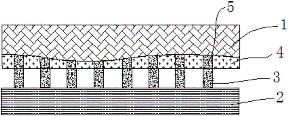
[0027] figure 1 A high-pixel infrared focal plane detector is shown, which includes interconnected mercury cadmium telluride epitaxial wafers 1 and a readout circuit 2, and the surface of the readout circuit 2 is prepared with a first flip-chip welding structure 3, cadmium telluride The surface of the mercury epitaxial wafer 1 is prepared with a second flip chip structure 5 matching the first flip chip structure 3, wherein the surface of the mercury cadmium telluride epitaxial wafer 1 is also covered with a layer of protective material 4, and the protective material 4 can be filled with glue or ZnS etc. cover the HgCdTe epitaxial wafer 1 with the second flip-chip bonding structure 5 exposed on the surface of the HgCdTe epitaxial wafer 1, and the readout circuit 2 and the HgCdTe epitaxial wafer 1 pass through the first flip-chip bonding structure 3 and the second flip chip structure 5 are connected.

Embodiment 2

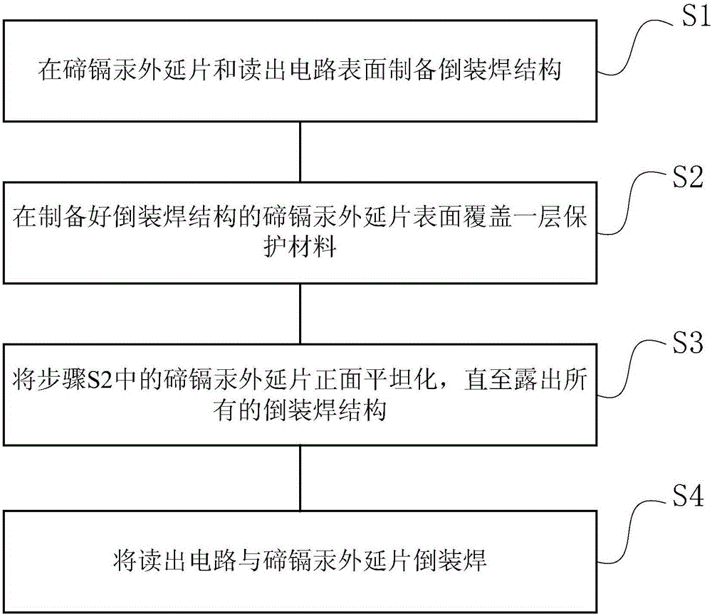
[0029] In this embodiment, a preparation method of a high-pixel infrared focal plane detector is also proposed, which is used to make the infrared focal plane detector in the embodiment, such as figure 2 shown, including the following steps:

[0030] S1. Prepare a flip-chip structure on the surface of the HgCdTe epitaxial wafer and the readout circuit;

[0031] S2. Covering a layer of protective material on the surface of the HgCdTe epitaxial wafer with the flip chip structure prepared;

[0032] S3, planarizing the front side of the HgCdTe epitaxial wafer in step S2 until all the flip chip structures are exposed;

[0033] S4. Flip-chip welding the readout circuit to the HgCdTe epitaxial wafer.

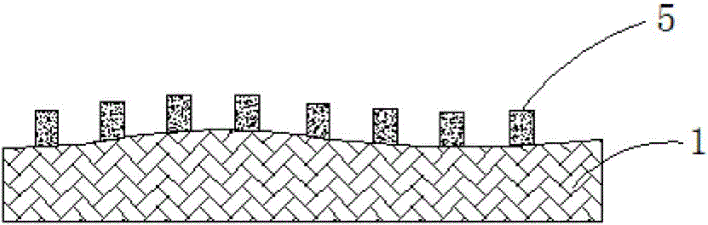
[0034] Specifically, according to the existing process technology, namely photolithography, coating and stripping, the second flip chip structure 5 is prepared on the HgCdTe epitaxial wafer 1 (such as image 3 As shown), the first flip-chip structure 3 is prepared on the readout ci...

Embodiment 3

[0036] In this implementation, steps are also included:

[0037] S1. Prepare a flip-chip structure on the surface of the HgCdTe epitaxial wafer and the readout circuit;

[0038] S2. Covering a layer of protective material on the surface of the HgCdTe epitaxial wafer with the flip chip structure prepared;

[0039] S3, planarizing the front side of the HgCdTe epitaxial wafer in step S2 until all the flip chip structures are exposed;

[0040] S4. Flip-chip welding the readout circuit to the HgCdTe epitaxial wafer.

[0041] Specifically, according to the existing technology, that is, photolithography, coating and stripping, the second flip-chip structure 5 is prepared on the HgCdTe epitaxial wafer 1, and the second flip-chip structure is prepared on the readout circuit 2 3. Then, a layer of ZnS with a thickness not lower than the second flip-chip structure is deposited on the surface of the HgCdTe epitaxial wafer 1 by means of electron beam evaporation to obtain the HgCdTe epit...


PUM


Abstract

The invention relates to a high-pixel infrared focal plane array detector and a preparation method thereof. The detector comprises a mercury cadmium telluride epitaxial wafer and a read-out circuit, which are connected with each other, wherein a flip-chip bonding structure is prepared on the surfaces of the read-out circuit and the mercury cadmium telluride epitaxial wafer; a protective material layer also covers the surface of the mercury cadmium telluride epitaxial wafer; a filling adhesive or ZnS and the like can be selected as the protective material; the flip-chip bonding structure exposed outside the surface of the mercury cadmium telluride epitaxial wafer covers the mercury cadmium telluride epitaxial wafer; and the read-out circuit is connected with the mercury cadmium telluride epitaxial wafer through the flip-chip bonding structure. The problem of surface roughness of the mercury cadmium telluride epitaxial wafer is solved through planarization; the flip-chip bonding yield is improved; and meanwhile, the material stress caused by roughness in the flip-chip bonding process is avoided.

Description

technical field [0001] The invention relates to the field of infrared focal plane detection, and more specifically relates to a high-pixel infrared focal plane detector and a preparation method thereof. Background technique [0002] Due to the special properties of the material and the immaturity of the current process, compared with the silicon-based technology, the surface of the HgCdTe epitaxial wafer has greater unevenness. Under the existing mercury cadmium telluride technology level, the epitaxial yield rate that meets the requirement that the height difference within an area of ​​1cm2 is less than 1um is very low. The unevenness of the surface will lead to the problem of bonding failure in the manufacture of infrared focal plane devices, especially for high-pixel detectors, which has a great impact and is one of the most important reasons for the low yield of flip-chip soldering. [0003] Compared with materials such as silicon, HgCdTe materials should not be planari...

Claims


Application Information

Patent Timeline
IPC IPC(8): H01L23/498H01L25/16H01L21/60
CPCH01L23/49811H01L23/49894H01L23/562H01L24/83H01L25/167H01L2224/83355
Inventor 金迎春黄立周文洪刘斌姚柏文戴俊碧骆鲁斌龚健
Owner WUHAN GAOXIN TECH
Why Eureka
Try Eureka