Field effect transistor and method of manufacturing the same

a field effect transistor and transistor technology, applied in the field of field effect transistors, can solve the problems of large leakage current and reduced off-breakdown voltage, and achieve the effect of increasing off-breakdown voltage and reducing off-breakdown voltag

Active Publication Date: 2011-11-10
PANASONIC CORP
View PDF5 Cites 31 Cited by
  • Summary
  • Abstract
  • Description
  • Claims
  • Application Information

AI Technical Summary

Benefits of technology

[0020]Also, in the case where the field-effect transistor is used as a power transistor, heat generation due to the leakage current is high, and consequently, the OFF-breakdown voltage is reduced.
[0021]In view of the above-mentioned existing problems, an object of the present invention is to provide a field-effect transistor as a normally-off semiconductor device including a nitride semiconductor, which allows the leakage current in OFF state to be suppressed and the OFF-breakdown voltage to be increased.

Problems solved by technology

However, the JFET including the conventional nitride semiconductor has a problem of a large leakage current and a reduced OFF-breakdown voltage in the off-state of the transistor.

Method used


Image

  • Field effect transistor and method of manufacturing the same
  • Field effect transistor and method of manufacturing the same
  • Field effect transistor and method of manufacturing the same

Examples


first embodiment

[0091]A first embodiment of the present invention is described with reference to the drawings.

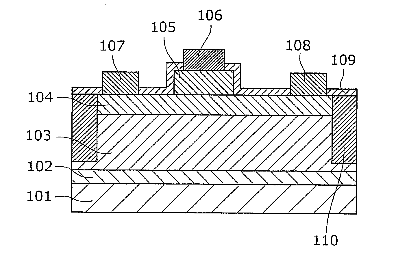
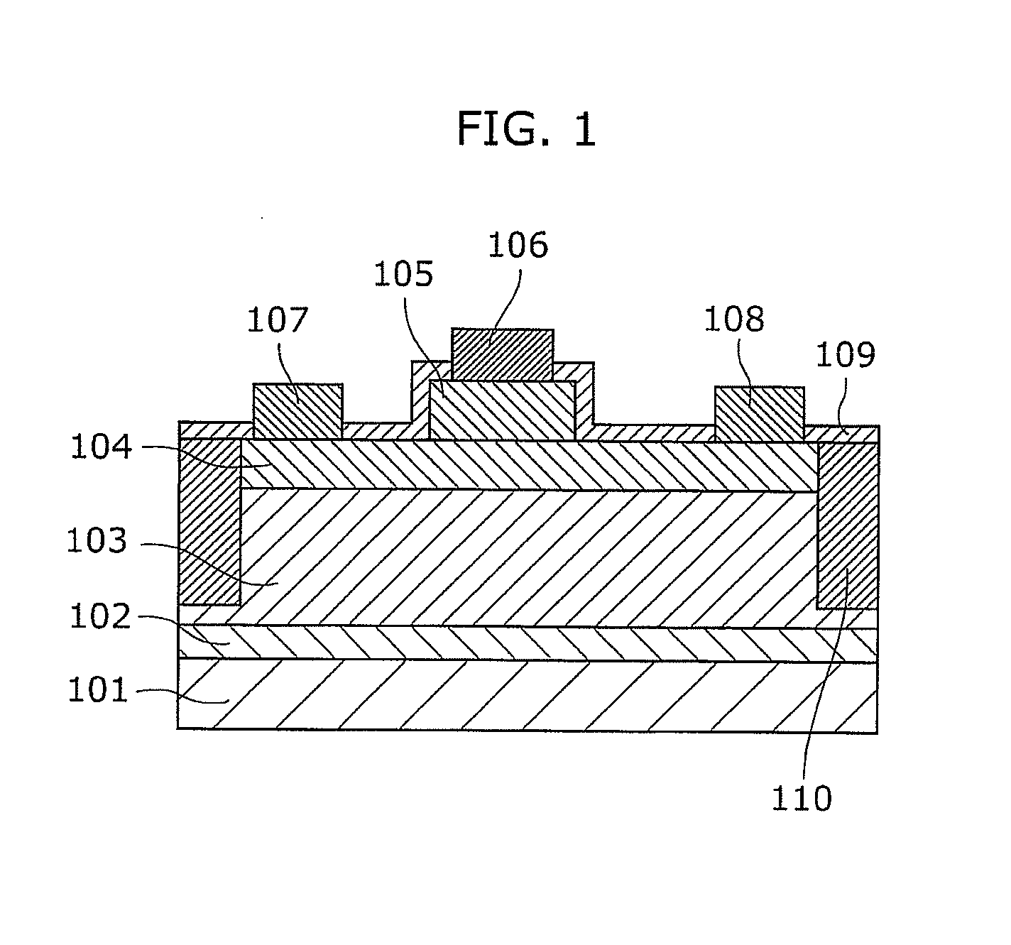
[0092]FIG. 1 shows a structural diagram of a sectional view of a field-effect transistor according to the first embodiment of the present invention. As shown in FIG. 1, the field-effect transistor according to the first embodiment includes a buffer layer 102 including aluminum nitride (AlN), having a film thickness of 100 nm, an undoped gallium nitride (GaN) layer 103 having a film thickness of 2 μm, an undoped aluminum gallium nitride (AlGaN) layer 104 having a film thickness of 25 nm, and a p-type AlGaN layer 105 having a film thickness of 50 nm that are sequentially formed by epitaxial growth on a sapphire substrate 101 including sapphire having the plane orientation of the (0001) plane. Here, the Al composition in each of AlGaN layers 104 and 105 is 20%. For the undoped GaN layer 103, AlxGa1-xN (where 0≦x≦1) may be used; for the undoped AlGaN layer 104, AlyGa1-yN (where 0105, AlzGa1-zN ...


PUM


Abstract

A field-effect transistor includes a first semiconductor layer formed on a substrate, and a second semiconductor layer. The first semiconductor layer has a containing region provided as an isolation region which contains non-conductive impurities, and a non-containing region which contains no non-conductive impurities. A first region is defined by a vicinity of a portion of the interface between the containing region and the non-containing region, the portion of the interface being below a gate electrode, the vicinity including the portion of the interface and being included in the containing region. The second semiconductor layer includes a second region which is located directly above the first region. The concentration of the non-conductive impurities of the second region is lower than that of the first region.

Description

CROSS REFERENCE TO RELATED APPLICATION[0001]This is a continuation application of PCT application No. PCT / JP2010 / 000232 filed on Jan. 18, 2010, designating the United States of America.BACKGROUND OF THE INVENTION[0002](1) Field of the Invention[0003]The present invention relates to a field effect transistor using a nitride semiconductor and a method of manufacturing the field effect transistor that can be applied to, for example, a power transistor used in a power supply circuit or the like of a consumer product.[0004](2) Description of the Related Art[0005]The group III nitride semiconductor represented by gallium nitride (GaN) is a wide-gap semiconductor, for which the band gaps of gallium nitride (GaN) and aluminum nitride (AlN) are wide, for example, 3.4 eV and 6.2 eV at room temperature, respectively, thus has a feature of high breakdown electric field and a higher electron saturation velocity than that of gallium arsenide (GaAs), silicon (Si) and the like. For this reason, fie...

Claims


Application Information

Patent Timeline
Patent Type & Authority Applications(United States)
IPC IPC(8): H01L29/80H01L21/335
CPCH01L29/1066H01L29/2003H01L29/7787H01L29/7783H01L29/66462
Inventor UMEDA, HIDEKAZUHIKITA, MASAHIROUEDA, TETSUZO
Owner PANASONIC CORP
Why Eureka
Try Eureka