Method of manufacturing semiconductor light-emitting device

a technology of light-emitting devices and semiconductors, which is applied in the manufacturing of semiconductor/solid-state devices, semiconductor devices, electrical devices, etc., can solve the problems of easy leakage of led chips, easy cleavage, and the rigidity of the apphire component commonly used as a substrate material of led chips, so as to prevent prevent leakage. , the effect of preventing the occurrence of chipping

Active Publication Date: 2011-11-10
TOYODA GOSEI CO LTD
View PDF0 Cites 27 Cited by
  • Summary
  • Abstract
  • Description
  • Claims
  • Application Information

AI Technical Summary

Benefits of technology

[0024]According to the above-mentioned configurations, it is possible to provide a method of manufacturing a semiconductor light-emitting device which is capable of preventing the occurrence of chipping when divided from a sapphire substrate, and preventing leakage even when chipping occurs.
[0025]According to the method of manufacturing a semiconductor light-emitting device of the present invention, since the first dividing groove is formed between the long sides of the light-emitting device sections so that the long side of the light-emitting device section is along the easily cleaved plane of the substrate, it is possible to easily cleave the substrate by the first dividing groove, and to prevent the occurrence of chipping in the long side of the light-emitting device section. In addition, since the second dividing groove having a larger width than the width of the first dividing groove is formed between the short sides of the light-emitting device sections, even when chipping occurs at the time of cleaving the substrate by the second dividing groove, chipping does not reach the light-emitting device section, thereby allowing leakage in the light-emitting device section to be prevented.

Problems solved by technology

In recent years, with the miniaturization and high performance of LED chips, an important issue has been raised regarding how many LED chips to cut out from one substrate without damaging the light-emitting device section of the LED chip in a scribing step.
However, a sapphire component commonly used as a substrate material of the LED chip is too rigid to be processed.
Therefore, even when the scribing method is used, small cracks are generated, and thus chipping often occurs.
When an n-type semiconductor layer, an active layer, a p-type semiconductor layer and the like are exposed due to the occurrence of chipping or poor separation, there may be a case where leakage occurs in the LED chip.
However, on the long side of the LED chip, since cleavage is not performed along the easily cleaved plane, there is a problem in that chipping or poor separation is generated.

Method used


Image

  • Method of manufacturing semiconductor light-emitting device
  • Method of manufacturing semiconductor light-emitting device
  • Method of manufacturing semiconductor light-emitting device

Examples


first embodiment

[0035]An example of a method of manufacturing a semiconductor light-emitting device which is an embodiment of the invention will be described.

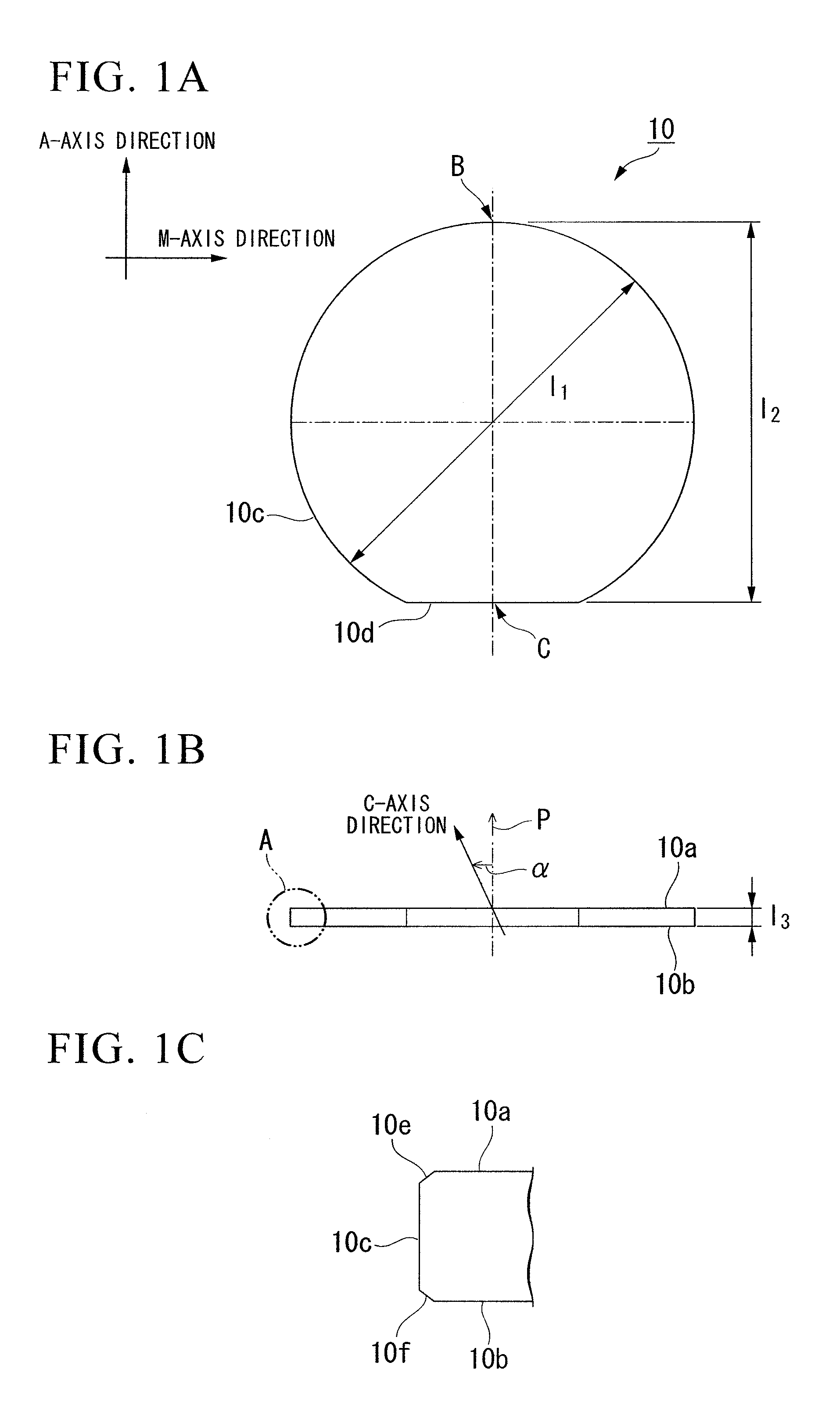
[0036]The method of manufacturing the semiconductor light-emitting device which is an embodiment of the invention includes the steps of forming a plurality of light-emitting device sections, having an approximately rectangular shape in a plan view, on a substrate in a matrix shape (first step), forming a first dividing groove between the long sides of the light-emitting device sections so that the long side of the light-emitting device section is along an easily cleaved plane of the substrate (second step), forming a second dividing groove, having a larger width than the width of the first dividing groove, between the short sides of the light-emitting device sections (third step), and dividing the substrate along the first dividing groove and the second dividing groove to cut out the light-emitting device section (fourth step).

[0037]Here, one ...

example 1

[0128]As shown below, a group-III nitride semiconductor light-emitting device having a light-emitting device section which includes a gallium nitride-based compound semiconductor was fabricated.

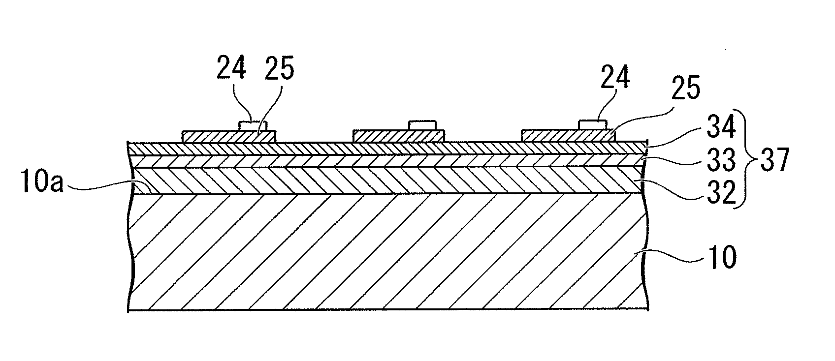
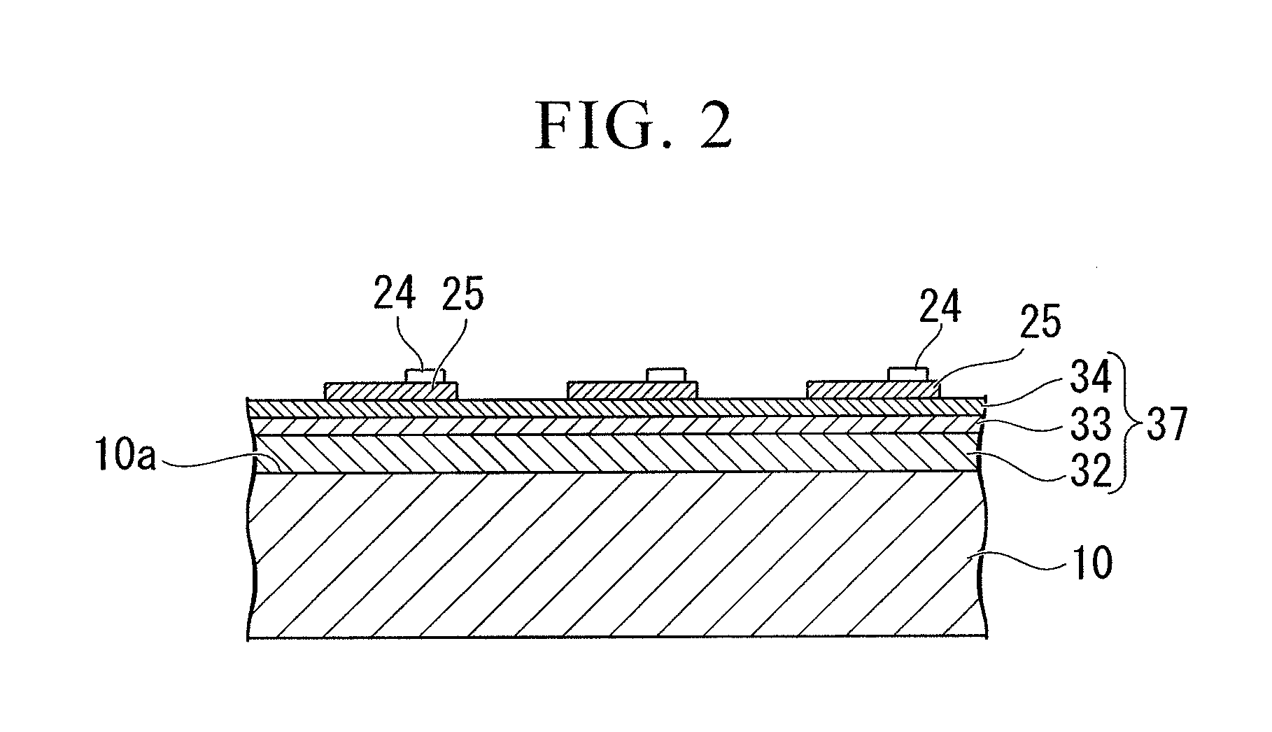
[0129]First, an underlying layer, made of undoped GaN, having a thickness of 4 μm, an n contact layer, made of Si-doped (concentration of 1×10¹⁹ / cm3) GaN, having a thickness of 2 μm, an n cladding layer, made of Si-doped (concentration of 1×10¹⁸ / cm3) In0.1Ga0.9N, having a thickness of 12.5 nm, a barrier layer, made of GaN, having a thickness of 16 nm, and a well layer, made of In0.2Ga0.8N, having a thickness of 2.5 nm were alternately laminated five times on the main plane of a disk-shaped C-plane sapphire substrate having an outside diameter of 100 mm with a buffer layer made of AlN interposed therebetween, and then an epitaxial layer, made of a group-III nitride semiconductor, having a thickness of 9 μm were finally formed in which a light-emitting layer, having a multiple quantum well stru...

examples 3 and 4

[0149]In the semiconductor light-emitting device according to Example 3, the sizes of the long side and the short side thereof, the arrangement of the semiconductor light-emitting device in the sapphire substrate, and the dividing groove widths were set to be the same as those of Example 1 except that the thickness of the sapphire substrate was reduced so that the total thickness of the semiconductor light-emitting device became 140 μm. In addition, in the semiconductor light-emitting device according to Example 4, the sizes of the long side and the short side of the semiconductor light-emitting device, the arrangement of the semiconductor light-emitting device in the sapphire substrate, and the dividing groove widths were set to be the same as those of Example 2 except that the thickness of the sapphire substrate was reduced so that the total thickness thereof became 140 μm.

[0150]Meanwhile, in each of the substrates used in Example 3 and Example 4, a substrate was used in which the...


PUM


Abstract

A method of manufacturing a semiconductor light-emitting device which includes the steps of forming a plurality of light-emitting device sections (40), having an approximately rectangular shape in plan view, on a substrate (10) in a matrix shape, forming a first dividing groove (61) between the long sides (41) of the light-emitting device sections (40) so that the long side (41) of the light-emitting device section (40) is along an easily cleaved plane of the substrate (10), forming a second dividing groove (62), having a larger width than the width of the first dividing groove (61), between short sides (42) of the light-emitting device sections (40), and dividing the substrate (10) along a first dividing groove (61) and a second dividing groove (62) to cut out the light-emitting device section (40).

Description

BACKGROUND OF THE INVENTION[0001]1. Field of the Invention[0002]The present invention relates to a method of manufacturing a semiconductor light-emitting device.[0003]This application claims the benefit of Japanese Patent Application No. 2009-287900, filed in the Japanese Patent Office on Dec. 18, 2009, the content of which is incorporated herein by reference.[0004]2. Description of the Related Art[0005]Generally, after a plurality of light-emitting device sections are formed by laminating a semiconductor layer, made of GaN or the like, on the surface of a large-scale and thin substrate and then forming an electrode section, LED (Light-Emitting Diode) chips are manufactured by dividing the substrate for each light-emitting device section mentioned above using a scribing method. In recent years, with the miniaturization and high performance of LED chips, an important issue has been raised regarding how many LED chips to cut out from one substrate without damaging the light-emitting d...

Claims


Application Information

Patent Timeline
Patent Type & Authority Applications(United States)
IPC IPC(8): H01L33/20
CPCH01L33/0095H01L33/007
Inventor OKABE, TAKEHIKO
Owner TOYODA GOSEI CO LTD
Why Eureka
Try Eureka