Coupled plasmonic waveguides and associated apparatuses and methods

a plasmonic waveguide and plasmonic waveguide technology, applied in the field of coupling plasmonic waveguides, can solve the problems of increasing the temperature to an unacceptable level, unable to spatially confine the optical spot as desired, and the field optics and dielectric waveguide structures enjoy high throughput, etc., and achieves the effect of managing the thermal load on the transducer and simple fabrication

Inactive Publication Date: 2011-11-17
CARNEGIE MELLON UNIV
View PDF7 Cites 8 Cited by
  • Summary
  • Abstract
  • Description
  • Claims
  • Application Information

AI Technical Summary

Benefits of technology

[0015]In contrast to the prior art, the present invention excites propagating plasmonic modes in a distributed fashion, allowing for smaller impedance mismatch at the point of spot localization. The present invention is also amenable to measurement of its plasmonic dispersion relationship, allowing the actual properties of the transducer to be measured relatively easily. With these measurements in hand, the dielectric illuminating structures can be tuned accordingly. Thus, this approach allows for the idea that the transducer need not have a specific shape, just a consistent one that can be deduced from a real fabricated device and matched or coupled with the dielectric waveguide. This may make for more robust design, fabrication and test cycles.
[0017]The present invention also offers advantages over the prior art including the ability to manage the thermal load on the transducer, relatively simple fabrication that is commercially attractive, and tolerance to manufacturing variations.

Problems solved by technology

This often results in a rather severe impedance mismatch and significant power dissipation in the rather small transducer, raising its temperature to an unacceptable level.
In contrast to near field devices and optical elements far field optics and dielectric waveguide structures enjoy high throughput but lack the ability to spatially confine the optical spot as desired.
However at sub-wavelength dimensions the efficiency of these structures can be quite poor.
Metallic structures can become difficult to analyze at optical frequencies as the perfect conductor approximation breaks down.
Real metals at optical frequencies exhibit complex dielectric behavior that is further complicated when shaping the metals into sub-wavelength structures.

Method used


Image

  • Coupled plasmonic waveguides and associated apparatuses and methods
  • Coupled plasmonic waveguides and associated apparatuses and methods
  • Coupled plasmonic waveguides and associated apparatuses and methods

Examples


Embodiment Construction

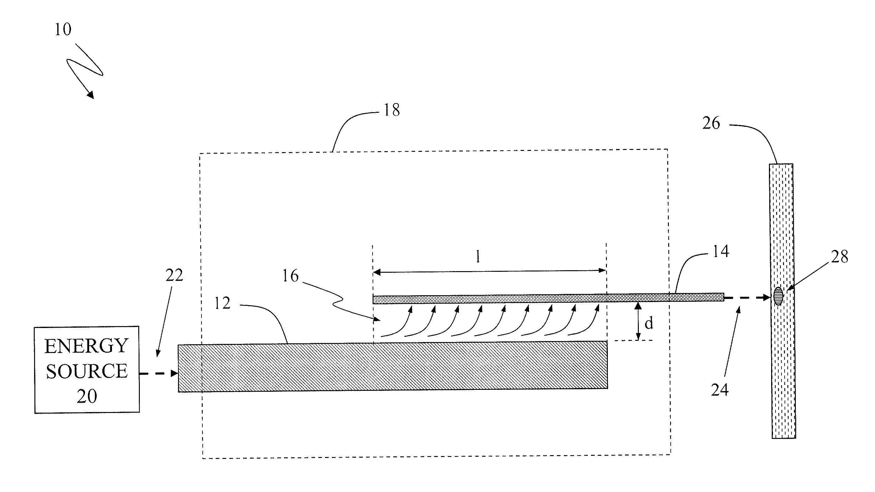
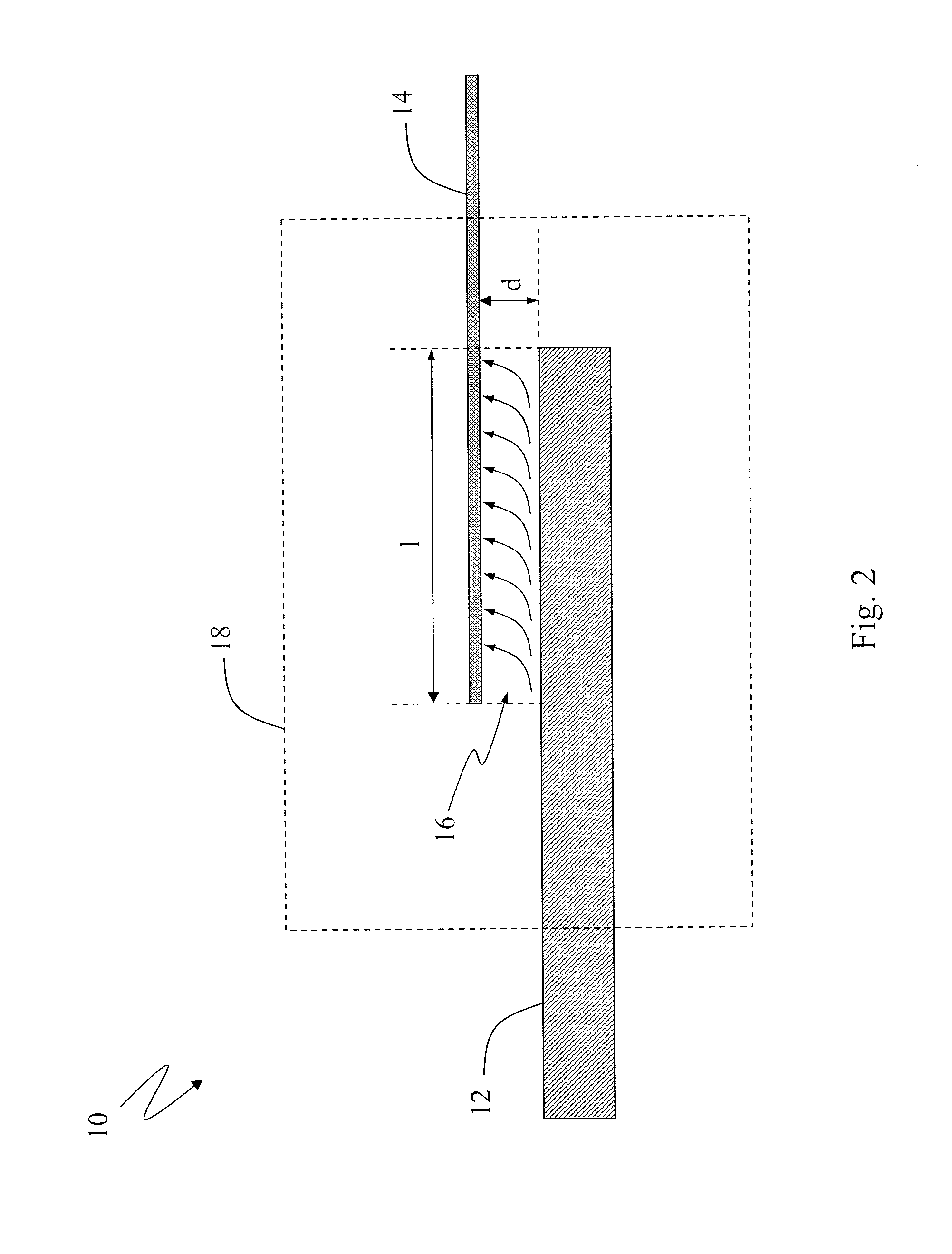
[0041]The present invention will generally be described in terms of coupled plasmonic waveguides and associated apparatuses and methods such as, for example, apparatuses and methods for coupled plasmonic waveguide transducers and near field optical sources. The present invention will also generally be described in terms of use in magnetic information storage devices, although the present invention is not limited to such devices and may be used with other applications such as, for example, generating small, intense optical spots for imaging or surface modification, or for other applications. Finally, the present invention includes many modifications and variations, and the specific descriptions and embodiments provided herein are illustrative of the present invention and not limiting. The present invention will be described in terms of both experimental examinations of the illumination structure and simulations of the near field transducer.

[0042]FIG. 2 illustrates one embodiment of a...


PUM


Abstract

An apparatus and corresponding method in which the apparatus includes a dielectric waveguide and a metallic waveguide. The dielectric waveguide has an effective mode index and a longitudinal dimension. The metallic waveguide has a longitudinal dimension and supports a surface plasmonic mode of propagation for a wavelength lambda. The metallic waveguide and the dielectric waveguide are adjacent to each other and overlap each other by a length along the longitudinal dimensions of both the dielectric waveguide and the metallic waveguide, wherein the length is greater than the wavelength lambda in the metallic waveguide. The metallic waveguide is coupled to the dielectric waveguide where the metallic waveguide and the dielectric waveguide overlap each other.

Description

CROSS-REFERENCE TO RELATED APPLICATIONS[0001]Not Applicable.STATEMENT REGARDING FEDERALLY-SPONSORED RESEARCH AND DEVELOPMENT[0002]Not Applicable.FIELD OF THE INVENTION[0003]The present invention is directed generally to coupled plasmonic waveguides and associated apparatuses and methods such as, for example, apparatuses and methods for coupled plasmonic waveguide transducers and near field optical sources.BACKGROUND OF THE INVENTION[0004]Optical near field writing (as in for example an information storage system that records data with the use of an optical spot) applications often require both high power throughput and well confined optical spots. There have been published papers describing a variety of near field transducers (“NFT”s) for confining light for applications including heat assisted magnetic recording. It has been proposed that these transducers can be illuminated with focused optical spots and with optical modes carried in waveguides. In most cases, though, the NFT is a...

Claims


Application Information

Patent Timeline
Patent Type & Authority Applications(United States)
IPC IPC(8): G02B6/42
CPCB82Y20/00G02F1/29G02B6/1226G11B5/314G11B2005/0021
Inventor BLACK, ERIC J.BAIN, JAMES A.POWELL, STEPHEN P.SCHLESINGER, TUVIAH E.
Owner CARNEGIE MELLON UNIV
Why Eureka
Try Eureka