Light-emitting semiconductor device

Inactive Publication Date: 2011-11-24
EPISTAR CORP
View PDF1 Cites 3 Cited by
  • Summary
  • Abstract
  • Description
  • Claims
  • Application Information

AI Technical Summary

Benefits of technology

[0006]One aspect of the present invention provides a light-e

Problems solved by technology

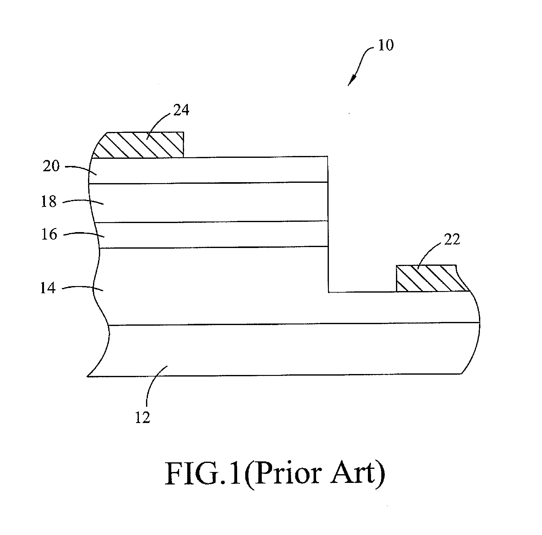
However, the lattice constant difference between the sapphire substrate 12 and the gallium nitride epitaxial layer is large, which generates defects in the epitaxial lay

Method used


Image

  • Light-emitting semiconductor device
  • Light-emitting semiconductor device
  • Light-emitting semiconductor device

Examples


Embodiment Construction

[0017]Reference will now be made in detail to the present preferred embodiments of the invention, examples of which are illustrated in the accompanying drawings. Wherever possible, the same reference numbers are used in the drawings and the description to refer to the same or like parts. In the drawings, the shape and thickness of an embodiment may be exaggerated for clarity and convenience. This description will be directed in particular to elements forming part of, or cooperating more directly with, apparatus in accordance with the present invention. It is to be understood that elements not specifically shown or described may take various forms well known to those skilled in the art. Further, when a layer is referred to as being on another layer or “on” a substrate, it may be directly on the other layer or on the substrate, or intervening layers may also be presented.

[0018]The preferred embodiments of the present invention will now be described in greater details by referring to t...


PUM


Abstract

The present invention provides a light-emitting semiconductor device, which comprises a substrate having a surface formed with a plane and a plurality of protrusions out of the plane. The plane is on a crystalline orientation. The protrusion is provided with an outer surface consisting of a plurality of sidewall surfaces. The sidewall surfaces are substantially not on the crystalline orientation. The protrusion is formed with an outline edge extended from the bottom to the top of the protrusion from a side view. The outline edge comprises at least one turning point. A first conductive type semiconductor layer is above the surface of the substrate, an active layer is above the first conductive type semiconductor layer, and a second conductive type semiconductor layer is above the active layer.

Description

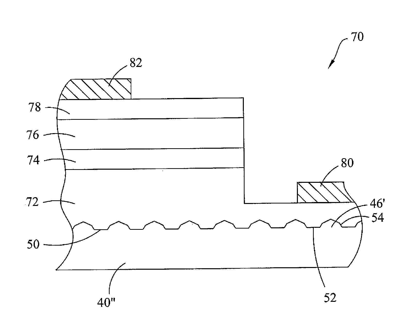
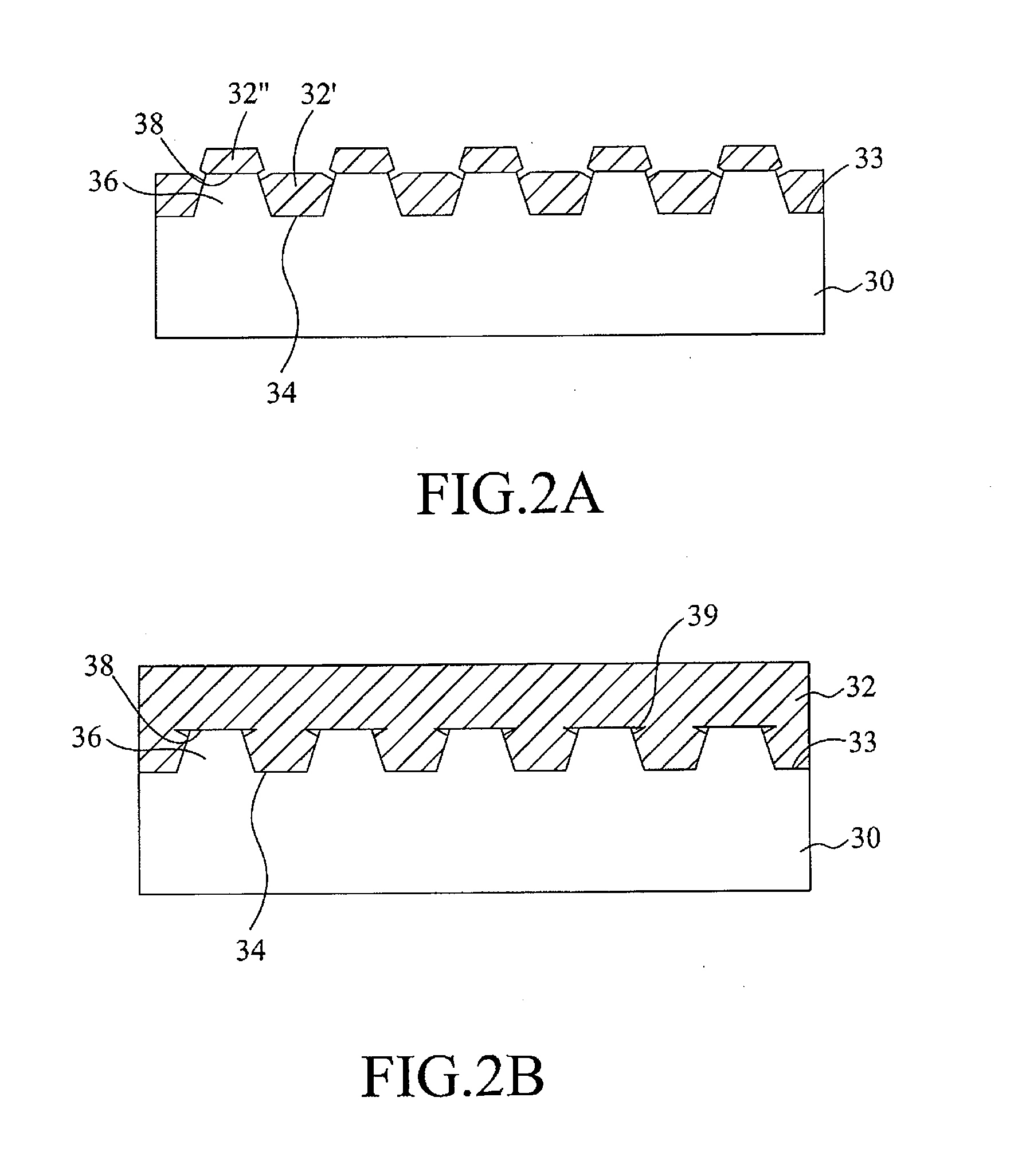
CROSS REFERENCE TO RELATED APPLICATIONS[0001]This application claims the right of priority based on Taiwan Patent Application No. 099116489 entitled “LIGHT-EMITTING SEMICONDUCTOR DEVICE,” filed on May 24, 2010, which is incorporated herein by reference and assigned to the assignee herein.FIELD OF INVENTION[0002]The present invention relates to light-emitting semiconductor devices, and more particularly, to a light-emitting semiconductor device having improved epitaxial quality and enhanced light extraction efficiency.BACKGROUND OF THE INVENTION[0003]The light emitting diode is a kind of various light-emitting semiconductor devices, which is advantageous with small volume, longevity, low voltage / current requirements, less fragile, less heat issues during emission, mercury-free, and low power consumption, and thus being extensively and widely used in many applications.[0004]FIG. 1 is a cross section of a conventional light emitting diode 10. Referring to FIG. 1, a light emitting diode...

Claims


Application Information

Patent Timeline
IPC IPC(8): H01L33/58
CPCH01L33/007H01L33/20H01L33/16
Inventor HSU, SHENG-HSIEN
Owner EPISTAR CORP
Why Eureka
Try Eureka