
asymmetric silicon-on-insulator (SOI) junction field effect transistor (JFET), a method of forming the asymmetrical soi jfet, and a design structure for the asymmetrical soi jfet

Active Publication Date: 2011-11-24
GLOBALFOUNDRIES US INC
View PDF2 Cites 27 Cited by
  • Summary
  • Abstract
  • Description
  • Claims
  • Application Information

AI Technical Summary

Benefits of technology

[0007]In another embodiment, the asymmetric SOI JFET can comprise a source-to-channel strap comprising a well region having the same conductivity type as the source and channel regions (i.e., the second conductivity type). This strap can extend vertically from the source region through the channel region to at least the bottom gate and, preferably, through the channel region and bottom gate to the insulator layer. Since the strap is only on the source side of the SOI JFET, it is non-annular with respect to the channel region. Such a strap provides improved link-up between the source and channel regions and, thereby reduces the on resistance of the SOI JFET.
[0011]In another embodiment, the method can comprise forming a source-to-channel strap comprising a well region having the same conductivity type as the source and channel regions (i.e., the second conductivity type). This strap can be formed such that it extends vertically from the source region down through the channel region to the bottom gate and, preferably, such that it extends vertically from the source region down through the channel region and the bottom gate to the insulator layer. Since the strap is formed so that it only extends from the source region, it is also formed so that it is non-annular with respect to the channel region. Such a strap provides improved link-up between the source and channel regions and, thereby reduces the on resistance of the SOI JFET.

Problems solved by technology

Such a non-annular gate contact provides a trade-off between the advantages of having a wrapped gate JFET and a lower resistance contact to the bottom gate with the disadvantage of having relatively large lateral dimensions.

Method used


Image

  •  asymmetric silicon-on-insulator (SOI) junction field effect transistor (JFET), a method of forming the asymmetrical soi jfet, and a design structure for the asymmetrical soi jfet
  •  asymmetric silicon-on-insulator (SOI) junction field effect transistor (JFET), a method of forming the asymmetrical soi jfet, and a design structure for the asymmetrical soi jfet
  •  asymmetric silicon-on-insulator (SOI) junction field effect transistor (JFET), a method of forming the asymmetrical soi jfet, and a design structure for the asymmetrical soi jfet

Examples


Embodiment Construction

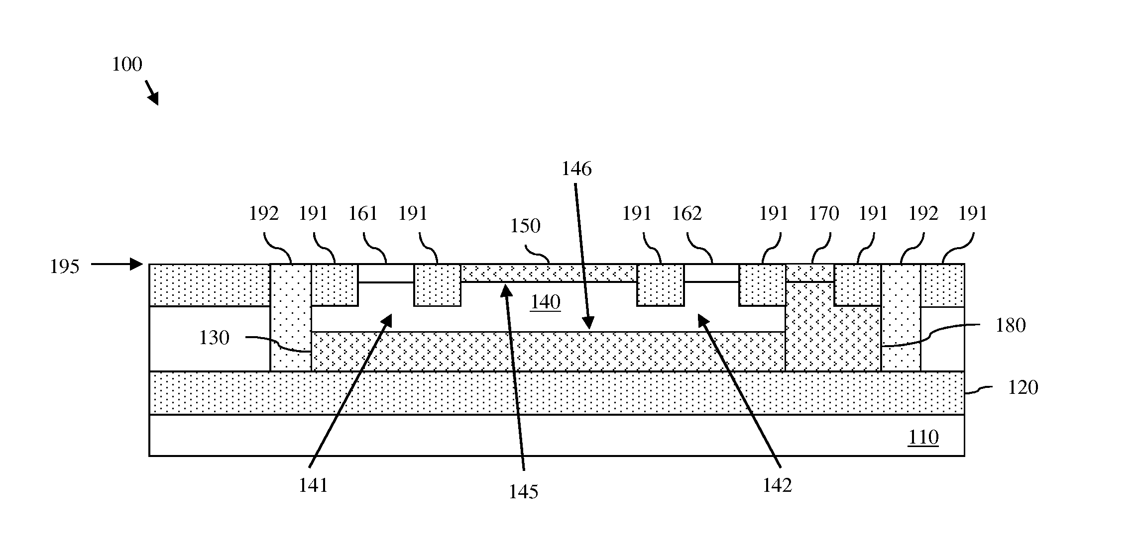
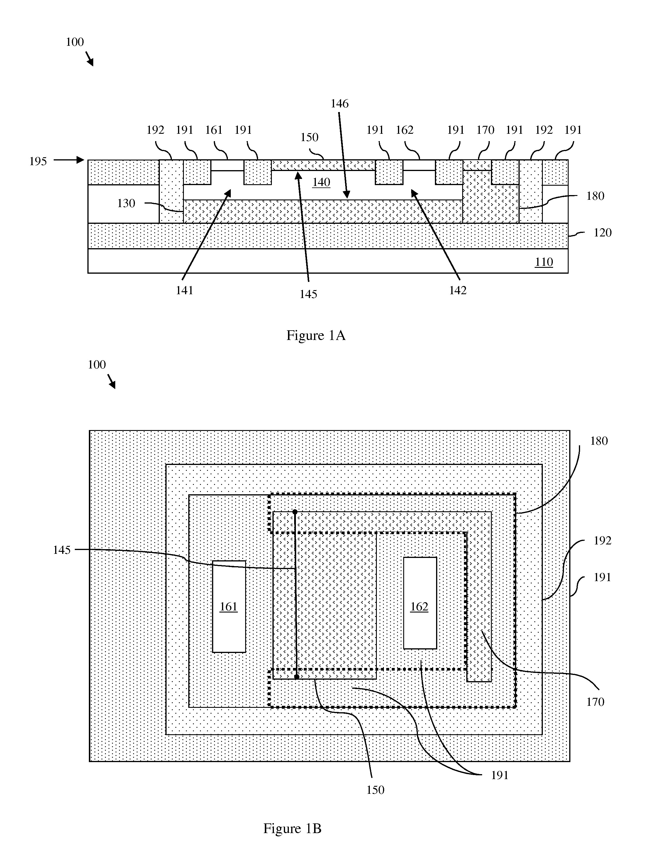
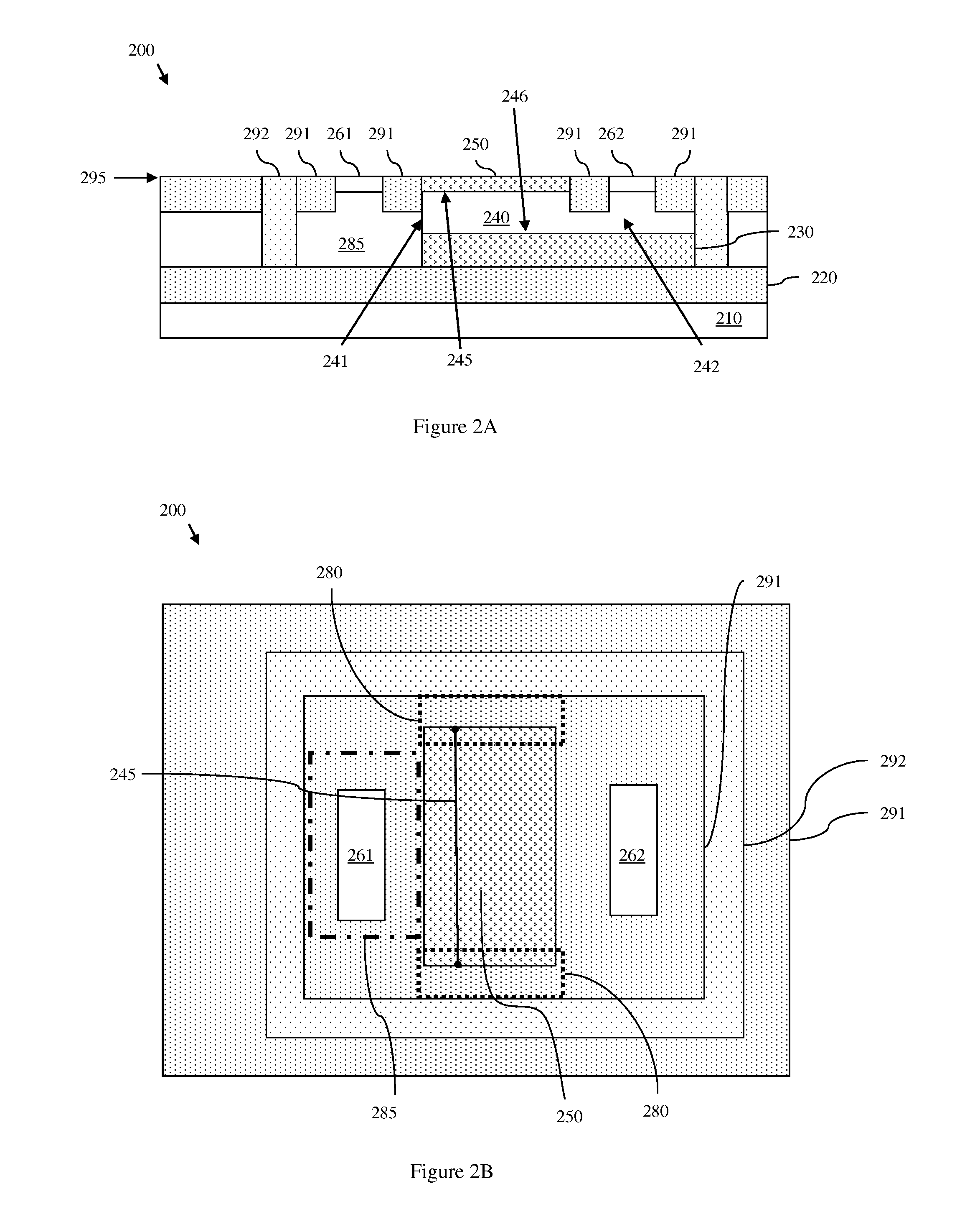
[0034]As mentioned above, recently, symmetric dual-gate and wrapped-gate junction field effect transistors (JFETs) have been developed. Advantages associated with symmetric dual-gate JFETs include a relatively large conduction area for a high on-current and tight channel region control for a low off-current, as compared to single-gate JFETs. Advantages associated with symmetric wrapped-gate JFETs include an even larger conduction area for a high on-current and even tighter channel region control for a low off-current. Unfortunately, a disadvantage associated specifically with symmetric, wrapped-gate, JFETs is the relatively large lateral dimensions, due to the multiple annular well regions. Furthermore, a disadvantage associated with both symmetric dual-gate and wrapped-gate JFETs (depending upon device performance requirements and specifications) is insufficient source-to-channel link-up. Thus, there is a need in the art for an improved JFET structure that balances the need for a r...


PUM


Abstract

An asymmetric silicon-on-insulator (SOI) junction field effect transistor (JFET) and a method. The JFET includes a bottom gate on an insulator layer, a channel region on the bottom gate and, on the channel region, source / drain regions and a top gate between the source / drain regions. STIs isolate the source / drain regions from the top gate and a DTI laterally surrounds the JFET to isolate it from other devices. Non-annular well(s) are positioned adjacent to the channel region and bottom gate (e.g., a well having the same conductivity type as the top and bottom gates can be connected to the top gate and can extend down to the insulator layer, forming a gate contact on only a portion of the channel region, and / or another well having the same conductivity type as the channel and source / drain regions can extend from the source region to the insulator layer, forming a source-to-channel strap).

Description

BACKGROUND[0001]1. Field of the Invention[0002]The embodiments relate to junction field effect transistors (JFETs), and more specifically, to an asymmetric semiconductor-on-insulator junction field effect transistor (SOI JFET), a method of forming such an asymmetric SOI JFET, and a design structure for the SOI JFET.[0003]2. Description of the Related Art[0004]Recently, symmetric dual-gate and wrapped-gate junction field effect transistors (JFETs) have been developed. Advantages associated with dual-gate JFETs include a relatively large conduction area for a high on-current and tight channel region control for a low off-current, as compared to single-gate JFETs. Advantages associated with wrapped-gate JFETs include an even larger conduction area for a high on-current and even tighter channel region control for a low off-current. However, there is a need in the art for improvements to these JFET structures in order to reduce lateral dimensions and / or optimize source-to-channel link-up...

Claims


Application Information

Patent Timeline
IPC IPC(8): H01L29/812H01L21/782G06F17/50H01L27/12
CPCG06F17/5068H01L21/84H01L29/8086H01L29/0843H01L29/66901H01L27/1203G06F30/39H01L29/0649
Inventor HERSHBERGER, DOUGLAS B.PHELPS, RICHARD A.RASSEL, ROBERT M.ST. ONGE, STEPHEN A.ZIERAK, MICHAEL J.
Owner GLOBALFOUNDRIES US INC
Features
  • Generate Ideas
  • Intellectual Property
  • Life Sciences
  • Materials
  • Tech Scout
  • Unparalleled Data Quality
  • Higher Quality Content
  • 60% Fewer Hallucinations
Learn More