Driving method of semiconductor device

a driving method and semiconductor technology, applied in static storage, digital storage, instruments, etc., can solve the problems of data stored in the semiconductor device that may change with time, and achieve the effect of suppressing the temporal change of data stored in the semiconductor device, suppressing the decrease of positive electric charge, and shortening the tim

Active Publication Date: 2011-11-24
SEMICON ENERGY LAB CO LTD
View PDF1 Cites 9 Cited by
  • Summary
  • Abstract
  • Description
  • Claims
  • Application Information

AI Technical Summary

Benefits of technology

[0019]A driving method of a semiconductor device according to one embodiment of the present invention includes a period (inverted period) in which a negative potential is applied to a gate of a transistor between a writing period and a retention period. In the inverted period, supply of positive electric charge from the drain of the transistor to an oxide semiconductor layer is promoted. Thus, accumulation of positive electric charge in the oxide semiconductor layer or at the interface between the oxide semiconductor layer and a gate insulating film can converge in a short time. Therefore, it is possible to suppress a decrease in the positive electric charge in the node electrically connected to the drain of the transistor in the retention period after the inverted period. That is, the temporal change of data stored in the semiconductor device can be suppressed.

Problems solved by technology

Thus, data stored in the semiconductor device may change with time.

Method used


Image

  • Driving method of semiconductor device
  • Driving method of semiconductor device
  • Driving method of semiconductor device

Examples


embodiment 1

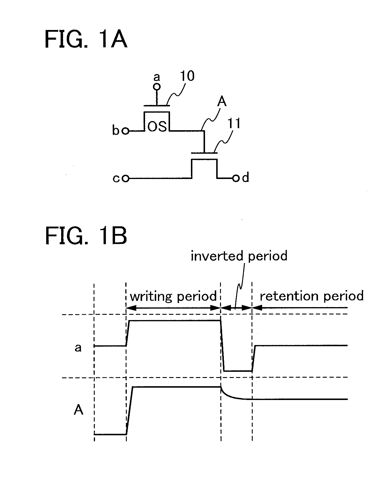
[0034]In this embodiment, an example of a semiconductor device which stores data by retaining electric charge in a node electrically connected to one of a source and a drain of a transistor whose channel region is included in an oxide semiconductor layer, and an example of a driving method of the semiconductor device will be described with reference to FIGS. 1A and 1B.

Example of Configuration

[0035]FIG. 1A is a circuit diagram of an example of a configuration of the semiconductor device according to this embodiment. The semiconductor device illustrated in FIG. 1A includes a transistor 10 and a transistor 11. A gate of the transistor 10 is electrically connected to a terminal a, and one of a source and a drain of the transistor 10 is electrically connected to a terminal b. A gate of the transistor 11 is electrically connected to the other of the source and the drain of the transistor 10, one of a source and a drain of the transistor 11 is electrically connected to a terminal c, and th...

embodiment 2

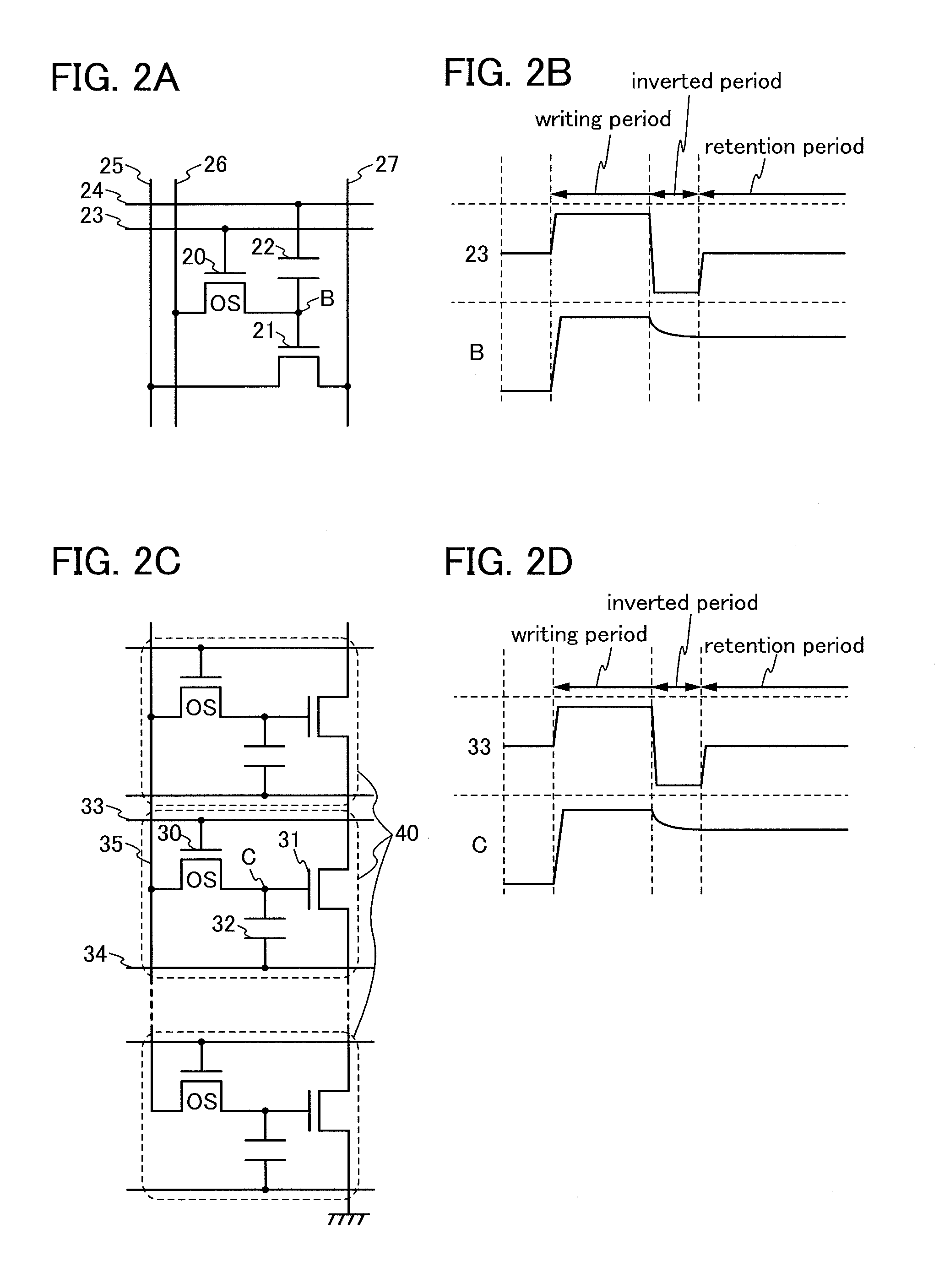
[0041]In this embodiment, specific examples of the semiconductor devices described in Embodiment 1 will be described with reference to FIGS. 2A to 2D.

specific example 1

[0042]FIG. 2A is a circuit diagram of a specific example of the semiconductor device described in Embodiment 1. The semiconductor device illustrated in FIG. 2A includes a transistor 20, a transistor 21, and a capacitor 22. A gate of the transistor 20 is electrically connected to a writing word line 23, and one of a source and a drain of the transistor 20 is electrically connected to a writing bit line 26. A gate of the transistor 21 is electrically connected to the other of the source and the drain of the transistor 20, one of a source and a drain of the transistor 21 is electrically connected to a reading bit line 25, and the other of the source and the drain of the transistor 21 is electrically connected to a fixed potential line 27. One electrode of the capacitor 22 is electrically connected to the other of the source and the drain of the transistor 20 and the gate of the transistor 21, and the other electrode of the capacitor 22 is electrically connected to a reading word line 2...


PUM


Abstract

A period (inverted period) in which a high negative potential is applied to a gate of the transistor is provided between a writing period and a retention period. In the inverted period, supply of positive electric charge from the drain of the transistor to the oxide semiconductor layer is promoted. Thus, accumulation of positive electric charge in the oxide semiconductor layer or at the interface between the oxide semiconductor layer and a gate insulating film can converge in a short time. Therefore, it is possible to suppress a decrease in the positive electric charge in the node electrically connected to the drain of the transistor in the retention period after the inverted period. That is, the temporal change of data stored in the semiconductor device can be suppressed.

Description

BACKGROUND OF THE INVENTION[0001]1. Field of the Invention[0002]The present invention relates to a driving method of a semiconductor device having transistors. Note that the semiconductor device in this specification indicates all the devices that operate by utilizing semiconductor characteristics.[0003]2. Description of the Related Art[0004]Storage devices using semiconductor elements are broadly classified into two categories: a volatile device that loses stored data when power supply stops, and a non-volatile device that retains stored data even when power is not supplied.[0005]A typical example of a volatile storage device is a dynamic random access memory (DRAM). A DRAM stores data in such a manner that a transistor included in a storage element is selected and electric charge is accumulated in a capacitor.[0006]When data is read from a DRAM, electric charge in a capacitor is lost on the above-described principle; thus, another writing operation is necessary every time data is ...

Claims


Application Information

Patent Timeline
Patent Type & Authority Applications(United States)
IPC IPC(8): G11C7/00
CPCG11C11/404G11C16/02G11C11/4076
Inventor KAMATA, KOICHIRO
Owner SEMICON ENERGY LAB CO LTD
Why Eureka
Try Eureka