Indium arsenide nanocrystals and methods of making the same

a nanocrystal and indium arsenide technology, applied in the field of nanocrystal materials, can solve the problems of out-performing other available biological labels, photoluminescence (pl), current limitations of these materials, etc., and achieve the effect of high photoluminescence (pl) and electroluminescence efficiency and stable against photo-oxidation

Inactive Publication Date: 2011-12-01
THE BOARD OF TRUSTEES OF THE UNIV OF ARKANSAS
View PDF0 Cites 1 Cited by
  • Summary
  • Abstract
  • Description
  • Claims
  • Application Information

AI Technical Summary

Benefits of technology

Core / shell semiconductor nanocrystals, in which the core composition differs from the composition of the shell that surrounds the core, are useful for many optical applications. If the band offsets of the core / shell structures are type-I, and the shell semiconductor possesses a larger bandgap than the core material, the photo-generated electron and hole inside a nanocrystal will be mostly confined within the core. As used herein, type-I band offsets refer to a core / shell electronic structure wherein both conduction and valence bands of the shell semiconductor are simultaneously either higher or lower than those of the core semiconductor. Consequently, conventional core / shell nanocrystals can show high photoluminescence (PL) and electroluminescence efficiencies and can be more stable against photo-oxidation than “plain core” semiconductor nanocrystals comprising a single material, provided that the bandgap of the core semiconductor is smaller than that of the shell semiconductor.

Problems solved by technology

Particularly, photoluminescent (PL) quantum dots having emission in the near-infrared (NIR) region of the electromagnetic spectrum (700-1400 nm) are likely out-perform other available biological labels for in-vivo imaging because of their large absorption cross section and narrow emission bands.
Nevertheless, the synthetic chemistry of semiconductor nanocrystals, including NIR emitting nanocrystals, is challenging and has inspired continuous efforts for developing high performance nanocrystals for use in various applications.
Generally speaking, current limitations of these materials include low emission efficiency, broad spectrum width, poor color control and / or poor stability.

Method used


Image

  • Indium arsenide nanocrystals and methods of making the same
  • Indium arsenide nanocrystals and methods of making the same
  • Indium arsenide nanocrystals and methods of making the same

Examples


example 1

As Prepared Monodisperse or Substantially Monodisperse InAs Nanocrystals

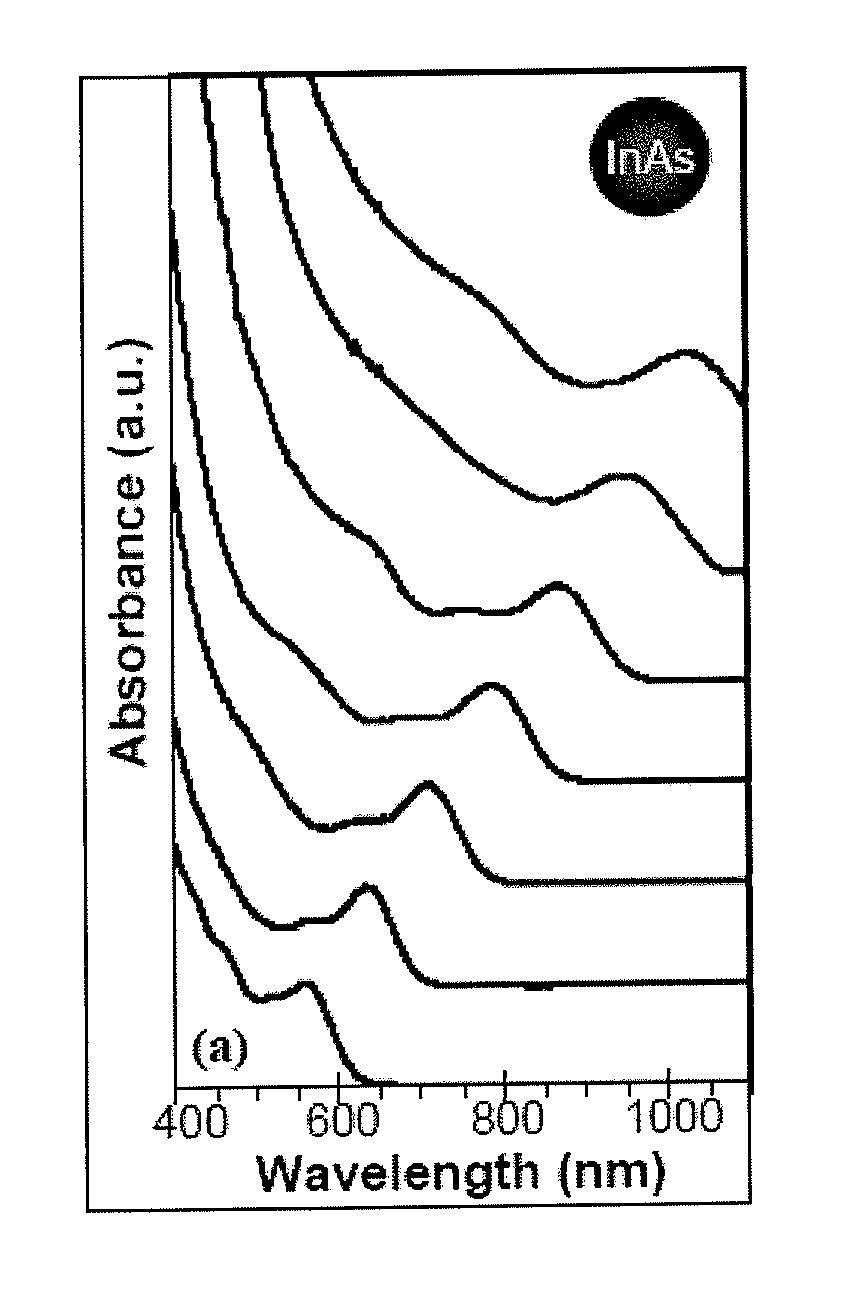
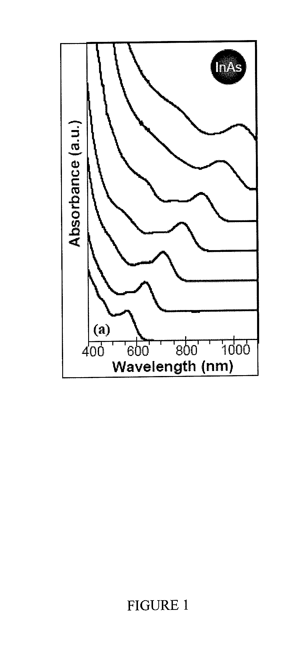
0.4 mM indium stearate, 0.5 ml TOP and 3.5 ml ODE were loaded into three-neck-flask. This mixture was heated to 150° C. under argon flow. An As(TMS)3 solution made in glovebox was subsequently injected into reaction mixture, and then the reaction mixture was heated up to 300° C. for the growth of monodisperse or substantially monodisperse InAs nanocrystals. To monitor the growth of the nanocrystals, aliquots were taken at different reaction times for absorption and emission measurement. FIG. 7 illustrates the as-prepared monodisperse or substantially monodisperse InAs nanocrystals of Example 1.

example 2

As Prepared Monodisperse or Substantially Monodisperse InAs / InP Nanocrystals

InAs core nanocrystals synthesized in Example 1 were cooled to 110° C. 0.3 mM stearic acid (0.5 ml in ODE) was injected into the reaction mixture. A mixture of 1 mM octylamine (0.2 ml) and 0.2 mM (TMS)3P in ODE (0.8 ml) was subsequently added into reaction mixture dropwise. After the addition of P precursor, the mixture was heated to 178° C. and maintained 45 minutes for the growth of InP shell onto the InAs core.

example 3

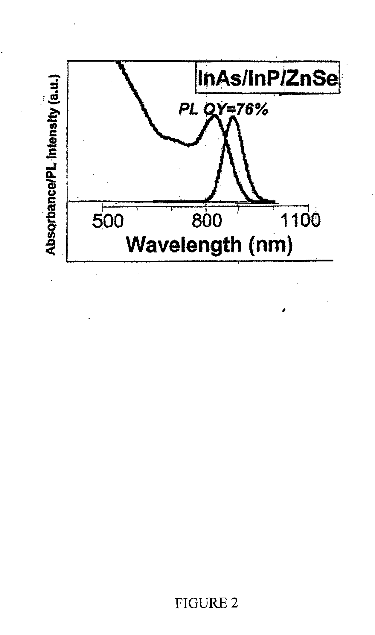
As Prepared Monodisperse or Substantially Monodisperse InAs / InP / ZnSe Core / Shell / Shell Nanocrystals

InAs core nanocrystals synthesized in Example 1 were cooled to 110° C. and 0.3 mM Stearic acid (0.5 ml in ODE) was injected into the reaction mixture. A mixture of 1 mM octylamine (0.2 ml) and 0.2 mM (TMS)3P in ODE (0.8 ml) was subsequently added to the reaction mixture dropwise. After the addition of P precursor, the mixture was heated to 178° C. and maintained 45 minutes for the growth of InP shell onto the InAs core.

Next, the same procedure was adopted for the growth of the ZnSe shell. When the indium precursor was depleted in the reaction mixture, 0.04 mM Se in TOP (0.2 ml) was injected into reaction vessel with InAs / InP nanocrystals. After 5 minutes, the same amount of zinc precursor was injected into reaction mixture. The temperature was subsequently increased to 220° C. for 30 mM to allow the growth of ZnSe shell. To monitor the growth of the nanocrystals, aliquots were taken at ...


PUM


Abstract

The present invention provides high quality monodisperse or substantially monodisperse InAs nanocrystals in the as-prepared state. In some embodiments, the as-prepared substantially monodisperse InAs nanocrystals demonstrate a photoluminescence of between about 700 nm and 1400 nm.

Description

FIELD OF THE INVENTIONThe present invention relates to nanocrystalline materials and, in particular, to nanocrystalline semiconductor materials and methods of making and using the same.BACKGROUND OF THE INVENTIONColloidal semiconductor nanocrystals or quantum dots have generated significant interest for their promise in developing advanced optical materials. Size-dependent emission is attractive property of semiconductor nanocrystals allowing their use in a variety of wavelength dependent applications.Biological labeling, for example, is expected to be a significant application of semiconductor nanocrystals. Particularly, photoluminescent (PL) quantum dots having emission in the near-infrared (NIR) region of the electromagnetic spectrum (700-1400 nm) are likely out-perform other available biological labels for in-vivo imaging because of their large absorption cross section and narrow emission bands. Moreover, semiconductor nanocrystals can also find significant application in displa...

Claims


Application Information

Patent Timeline
Patent Type & Authority Applications(United States)
IPC IPC(8): C09K11/74G01N15/02C22C28/00B22F9/16B82Y99/00
CPCC09K11/02Y10T428/2982C09K11/7492
Inventor PENG, XIAGANGXIE, RENGUO
Owner THE BOARD OF TRUSTEES OF THE UNIV OF ARKANSAS
Why Eureka
Try Eureka