Package systems having interposers

a technology of interposers and packaging systems, applied in the direction of semiconductor devices, semiconductor/solid-state device details, electrical apparatus, etc., can solve the problems of minimum size needed to make these components, physical limits of the density that can be achieved in two dimensions, and the requirement of more complex designs

Active Publication Date: 2011-12-01
TAIWAN SEMICON MFG CO LTD
View PDF33 Cites 541 Cited by
  • Summary
  • Abstract
  • Description
  • Claims
  • Application Information

AI Technical Summary

Problems solved by technology

Although dramatic improvements in lithography have resulted in considerable improvements in 2D integrated circuit formation, there are physical limits to the density that can be achieved in two dimensions.
One of these limits is the minimum size needed to make these components.
Also, when more devices are put into one chip, m

Method used


Image

  • Package systems having interposers
  • Package systems having interposers
  • Package systems having interposers

Examples


Embodiment Construction

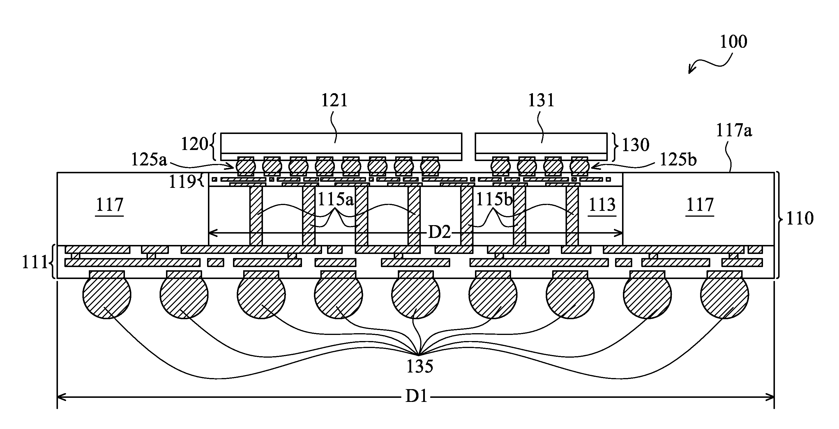
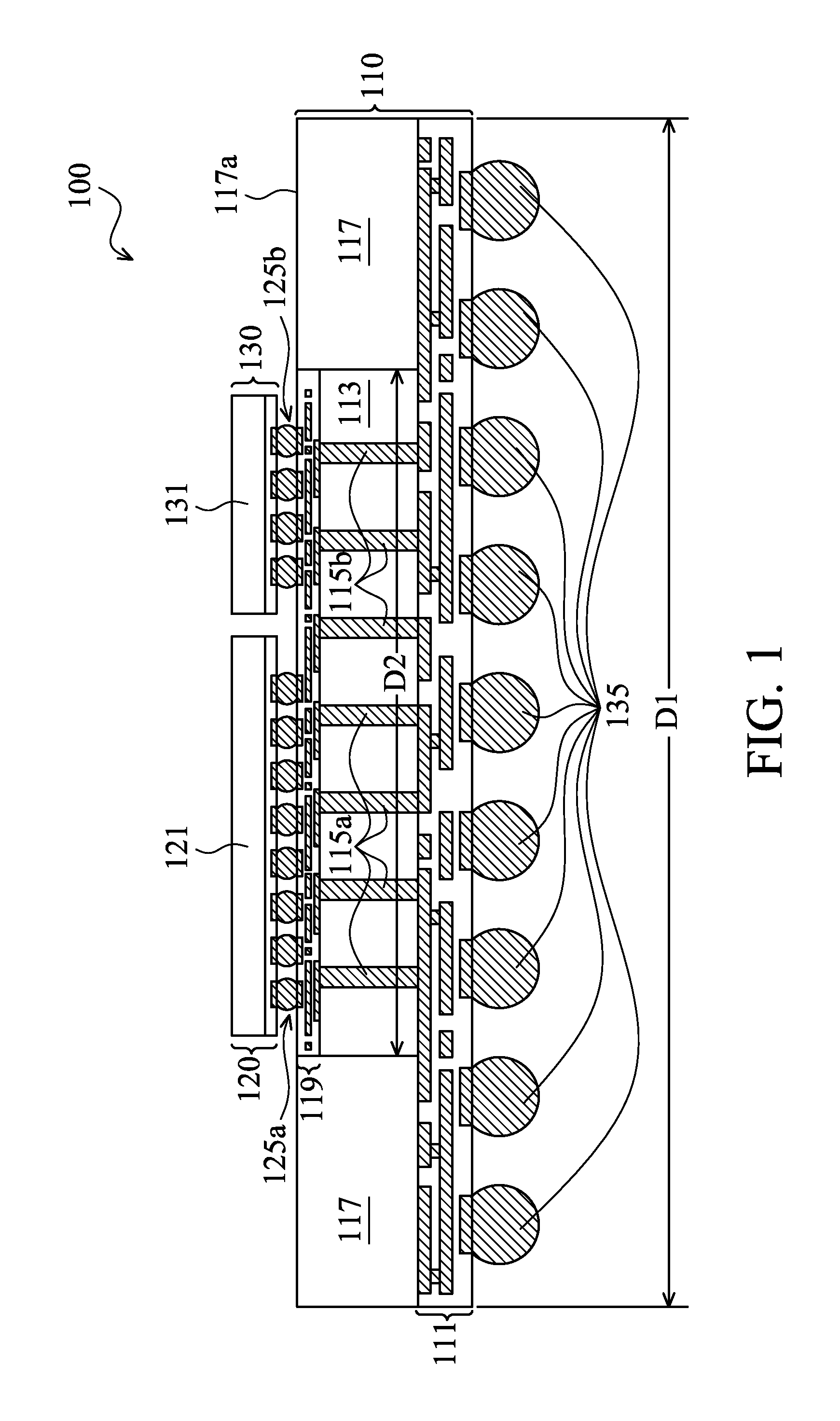
[0018]A package system has a silicon die directly disposed on an organic substrate that is disposed on a motherboard. The organic substrate serves as an intermediate apparatus to fan out the metal pitch of the silicon die to the metal pitch of the motherboard. It is found that a coefficient of thermal expansion (CTE) mismatch exists between the silicon die and the organic substrate. The CTE mismatch may result in an intermetal dielectric (IMD) layer delamination of the silicon die and / or a bump failure during an assembly process and / or a reliability test.

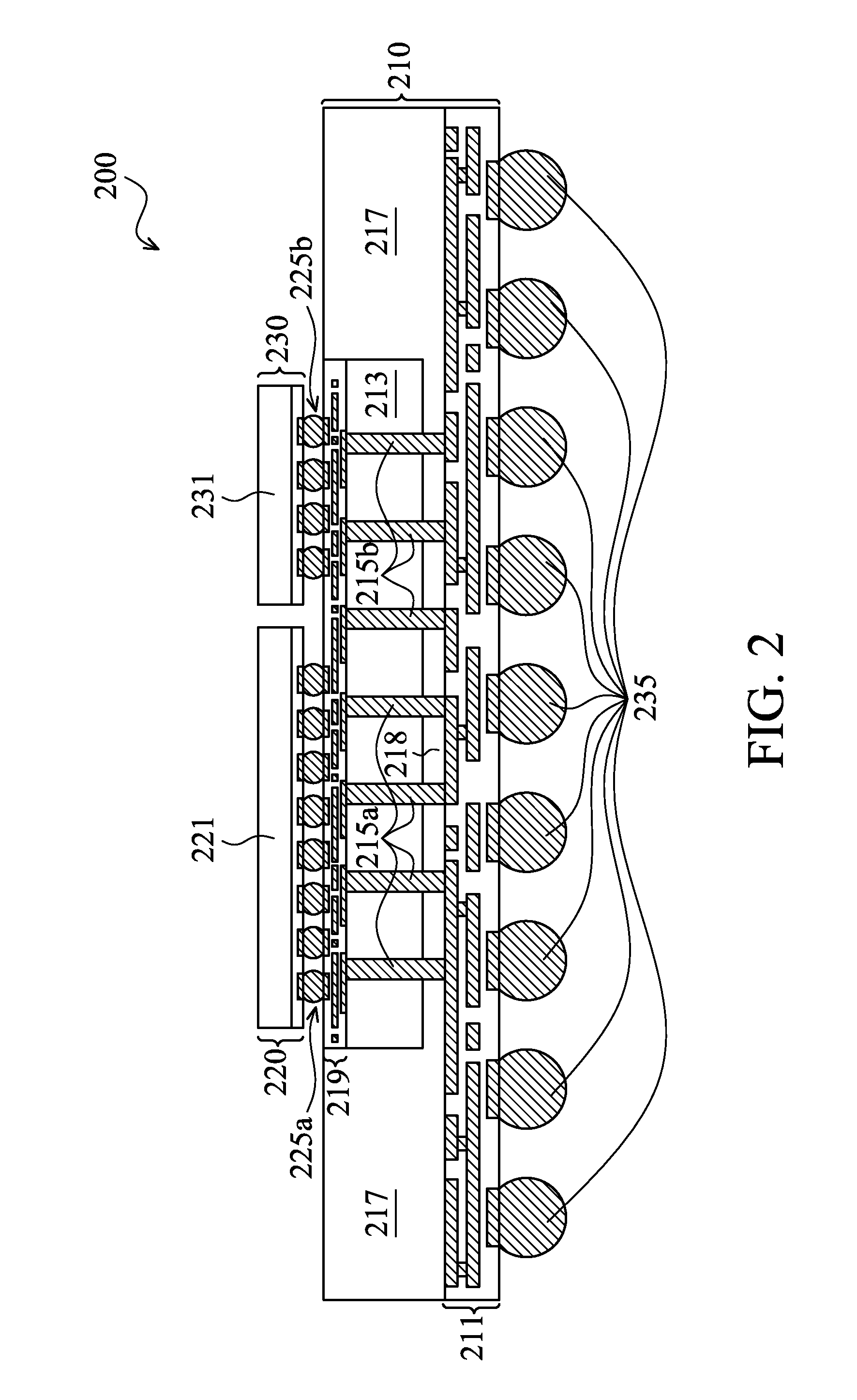
[0019]To solve the problem, a silicon interposer is disposed between the silicon die and the organic substrate, serving as another transition apparatus. The use of the silicon interposer increases the cost of manufacturing the package system. It is also found that the height of the package system with the silicon interposer is increased, too.

[0020]Based on the foregoing, package systems for integrated circuits are desired.

[0021]It i...


PUM


Abstract

A package system includes an integrated circuit disposed over an interposer. The interposer includes a first interconnect structure. A first substrate is disposed over the first interconnect structure. The first substrate includes at least one first through silicon via (TSV) structure therein. A molding compound material is disposed over the first interconnect structure and around the first substrate. The integrated circuit is electrically coupled with the at least one first TSV structure.

Description

RELATED APPLICATIONS[0001]The present application is related to U.S. patent application Ser. No. ______, entitled “PACKAGE SYSTEMS HAVING INTERPOSERS,” filed on ______ (Attorney Docket No. T5057-R220 (TSMC2010-0138)), which is incorporated herein by reference in its entirety.TECHNICAL FIELD[0002]The present disclosure relates generally to the field of semiconductor package systems, and more particularly, to package systems having interposers.BACKGROUND OF THE DISCLOSURE[0003]Since the invention of integrated circuits, the semiconductor industry has experienced continual rapid growth due to continuous improvements in the integration density of various electronic components (i.e., transistors, diodes, resistors, capacitors, etc.). For the most part, this improvement in integration density has come from repeated reductions in minimum feature size, allowing for the integration of more components into a given area.[0004]These integration improvements are essentially two-dimensional (2D) ...

Claims


Application Information

Patent Timeline
IPC IPC(8): H01L23/538
CPCH01L23/3128H01L23/49816H01L2924/1305H01L2924/13091H01L2924/10253H01L2924/01019H01L2224/16225H01L23/49827H01L23/49833H01L25/0652H01L25/0655H01L25/50H01L2224/16227H01L2924/15311H01L2924/00H01L2224/05573H01L24/16H01L21/486H01L21/565H01L21/76877H01L21/76895H01L24/11H01L24/81H01L25/0657H01L2224/11002H01L2224/16146H01L2225/06517H01L2225/06541H01L2225/06548H01L2225/06572H01L2924/14H01L2924/381H01L24/17H01L2224/05624H01L2924/00014H01L2224/05647H01L2224/05655H01L2224/05666H01L2224/05681H01L2224/05684
Inventor WU, WEI-CHENGHOU, SHANG-YUNJENG, SHIN-PUUYU, CHEN-HUA
Owner TAIWAN SEMICON MFG CO LTD
Why Eureka
Try Eureka