Crystalline semiconductor film manufacturing method, substrate coated with crystalline semiconductor film, and thin-film transistor

a technology of crystalline semiconductor film and manufacturing method, which is applied in the direction of semiconductors, electrical devices, transistors, etc., can solve the problems of loss of flatness, inability to obtain high-precision images, and inability to meet the requirements of the substrate, so as to achieve favorable in-plane uniformity

Inactive Publication Date: 2011-12-08
JOLED INC +1
View PDF3 Cites 7 Cited by
  • Summary
  • Abstract
  • Description
  • Claims
  • Application Information

AI Technical Summary

Benefits of technology

[0017]The present invention can implement a method of manufacturing a crystalline semiconductor film having a crystal structure with f...

Problems solved by technology

Moreover, a volume expansion in a crystallization process of the amorphous semiconductor film, that is, the volume expansion from liquid (in the melted state) to solid (in the crystallized state) causes protrusions on the surface of the crystallized crystalline semiconductor film, resulting in a loss of flatness.
This variation becomes a problem in a process, such as an etching process, to manufacture a thin-film transistor.
Also, a multiple number of beam shots are required to counter the in-plane variation of the crystallized crystalline semiconductor film, a...

Method used


Image

  • Crystalline semiconductor film manufacturing method, substrate coated with crystalline semiconductor film, and thin-film transistor
  • Crystalline semiconductor film manufacturing method, substrate coated with crystalline semiconductor film, and thin-film transistor
  • Crystalline semiconductor film manufacturing method, substrate coated with crystalline semiconductor film, and thin-film transistor

Examples


first embodiment

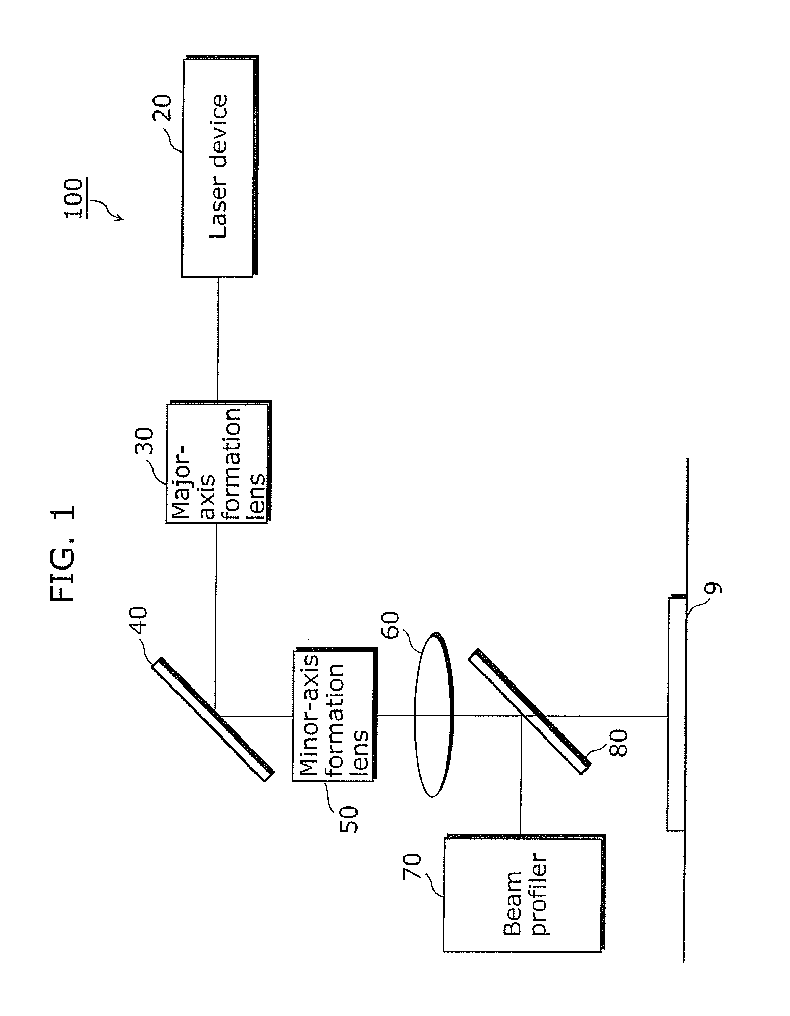
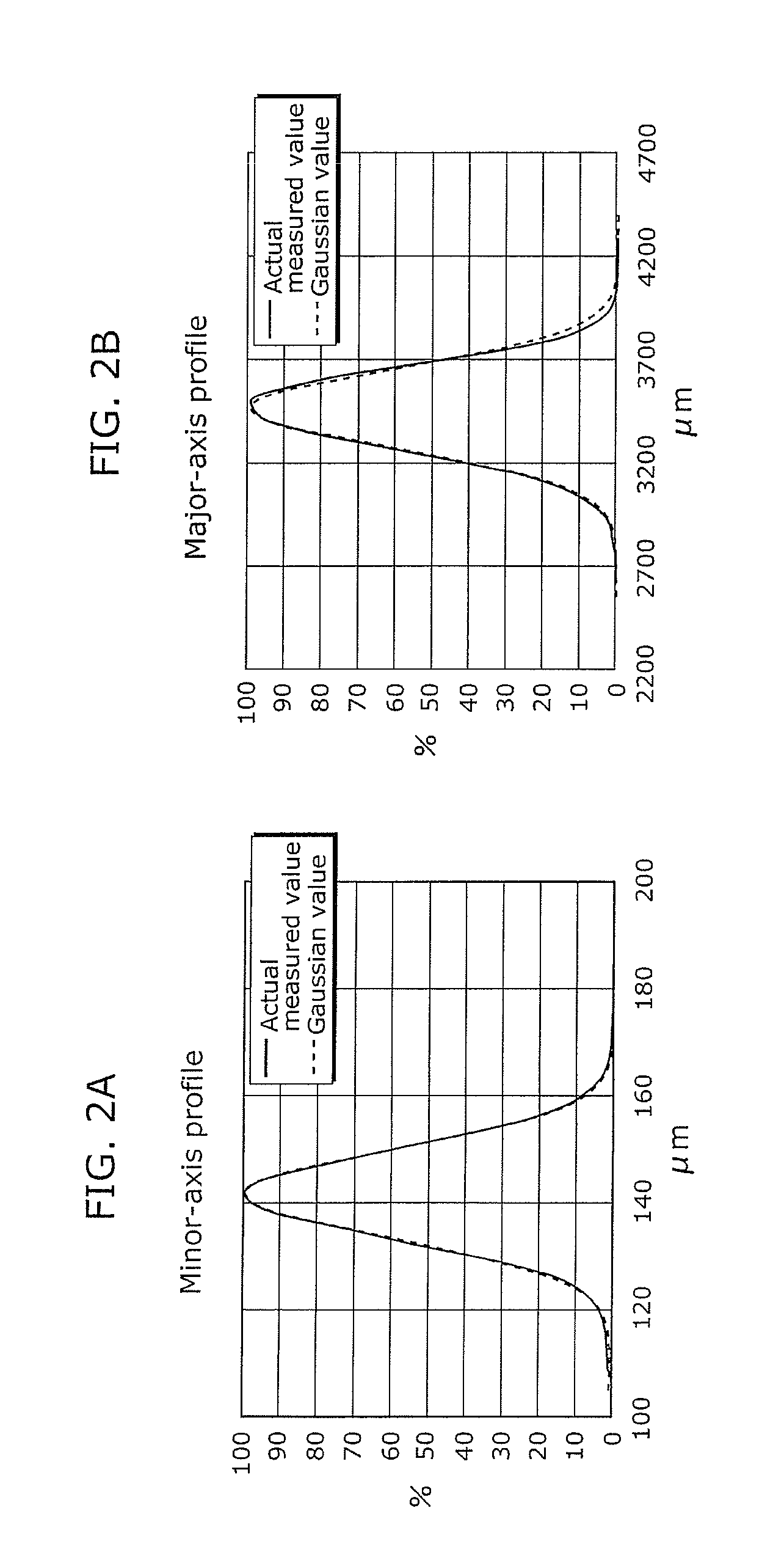
[0079]FIG. 1 is a diagram showing an example of a configuration of a CW laser crystallization device in the present embodiment. FIG. 2A is a diagram showing a minor-axis profile of a CW laser beam in the present embodiment. FIG. 2B is a diagram showing a major-axis profile of the CW laser beam in the present embodiment. Hereafter, the direction of the major axis is also referred to as the “longitudinal” direction.

[0080]A CW laser crystallization device 100 shown in FIG. 1 emits a CW laser beam onto a sample 9 which is an amorphous semiconductor, such as an amorphous silicon layer, formed on a glass substrate. The sample 9 is irradiated with the CW laser beam for a period of time on the order of microseconds. The CW laser crystallization device 100 includes a laser device 20, a major-axis formation lens 30, a mirror 40, a minor-axis formation lens 50, a condenser lens 60, a beam profiler 70, and a quartz glass 80.

[0081]The laser device 20 emits a CW laser beam. The laser device 20 em...

second embodiment

[0119]The second embodiment describes an example of the application of the crystalline semiconductor film having the crystal structure with favorable in-plane uniformity that is manufactured according to the method in the first embodiment.

[0120]FIG. 9 is a diagram explaining an example of the application of the crystalline semiconductor film to a substrate, in the present embodiment.

[0121]Firstly, a substrate coated with an amorphous semiconductor film and a longitudinal Gaussian CW laser beam are prepared. The substrate is configured with a base material 200 and an amorphous semiconductor film 210 which is formed on the base material 200. Here, a beam profile of the longitudinal Gaussian CW laser beam has a Gaussian light intensity distribution as shown in (a) of FIG. 9.

[0122]Next, the amorphous semiconductor film 210 is irradiated with the longitudinal Gaussian CW laser beam for a period of time on the order of microseconds. To be more specific, the amorphous semiconductor film 21...

third embodiment

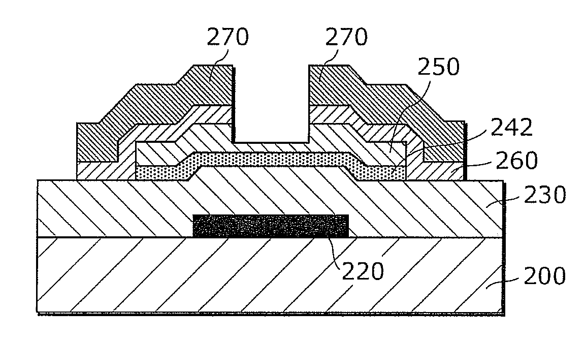
[0146]In the second embodiment, the bottom-gate thin-film transistor and the substrate coated with the crystalline semiconductor film are described as the application examples. The third embodiment describes a top-gate thin-film transistor as an application example.

[0147]FIG. 14 is a diagram explaining a method of manufacturing the top-gate thin-film transistor in the present embodiment. FIG. 15 is a diagram showing a configuration of the top-gate thin-film transistor in the present embodiment.

[0148]FIG. 14 shows a part of the process of manufacturing the top-gate thin-film transistor.

[0149]More specifically, (b) in FIG. 14 shows a manufacturing process of forming a source-drain electrode 310 on a base substrate 300 and then forming an amorphous semiconductor film 320 on the source-drain electrode 310. Following this, the amorphous semiconductor film 320 is irradiated with a longitudinal Gaussian CW laser beam shown in (a) of FIG. 14, and is then crystallized as shown in (c) of FIG....


PUM


Abstract

To provide a method of manufacturing a crystalline semiconductor film having a crystal structure with favorable in-plane uniformity. The method includes: irradiating an amorphous semiconductor film with a continuous-wave laser beam to increase a temperature of the amorphous semiconductor film to a range of 600° C. to 1100° C., the continuous-wave laser beam having a light intensity distribution continuously convex upward on each of major and minor axes; crystallizing the amorphous semiconductor film at the temperature increased to the range of 600° C. to 1100° C.; and increasing a crystal grain size of the crystallized amorphous semiconductor film, as a result of an increase in an in-plane temperature of the crystallized amorphous film to a range of 1100° C. to 1414° C. by latent heat released in the crystallizing of the amorphous semiconductor film.

Description

CROSS REFERENCE TO RELATED APPLICATION[0001]This is a continuation application of PCT application No. PCT / JP2010 / 003157 filed on May 10, 2010, designating the United States of America.BACKGROUND OF THE INVENTION[0002](1) Field of the Invention[0003]The present invention relates to a method of manufacturing a crystalline semiconductor film, a method of manufacturing a substrate coated with a crystalline semiconductor film, and a thin-film transistor.[0004](2) Description of the Related Art[0005]Examples used for manufacturing a liquid crystal panel or an organic electroluminescence (EL) panel designed for a display device include a thin-film transistor (TFT). A semiconductor layer which is made of, for example, silicon and serves as a channel part of the thin-film transistor is formed, in general, from an amorphous semiconductor film or a crystalline semiconductor film. It is preferable that a semiconductor film serving as the channel part of the thin-film transistor be formed from a...

Claims


Application Information

Patent Timeline
IPC IPC(8): H01L29/786H01L21/336
CPCH01L21/02532H01L27/1285H01L27/1281H01L21/02683H01L21/02675H01L27/1214
Inventor KATO, TOMOYAODA, TOMOHIKOOOTAKA, SEI
Owner JOLED INC
Why Eureka
Try Eureka