Deep ultraviolet light emitting diode

a technology of ultraviolet light and diodes, which is applied in the field of nitride-based heterostructures, can solve the problems of inhomogeneous al composition and lateral phase separation, low external quantum efficiency and wall plug efficiency of typical duv leds, and low internal quantum efficiency

Active Publication Date: 2011-12-22
SENSOR ELECTRONICS TECH
View PDF5 Cites 35 Cited by
  • Summary
  • Abstract
  • Description
  • Claims
  • Application Information

AI Technical Summary

Benefits of technology

[0011]Additional aspects of the invention provide methods of designing and / or fabricating the heterostructures and devices shown and described herein, as well as methods of designing and / or fabricating circuits including such devices, and the resulting circuits. The illustrative aspects of the invention are designed to solve one or more of the problems herein described and / or one or more other problems not discussed.

Problems solved by technology

However, external quantum efficiency and wall plug efficiency of typical DUV LEDs is below three percent, with the highest efficiencies for 280 nm LEDs and lower efficiencies for LEDs emitting ultraviolet light having shorter wavelengths.
In UV LEDs emitting ultraviolet light having a shorter wavelength, the internal quantum efficiency also drops due to materials problems resulting from growth of AlGaN structures with high Al content.
Such growth, among other things, is complicated by the low mobility of Al adatoms, which can result in inhomogeneous Al composition and lateral phase separation, as well as high density of threading dislocations and point defects.

Method used


Image

  • Deep ultraviolet light emitting diode
  • Deep ultraviolet light emitting diode
  • Deep ultraviolet light emitting diode

Examples


Embodiment Construction

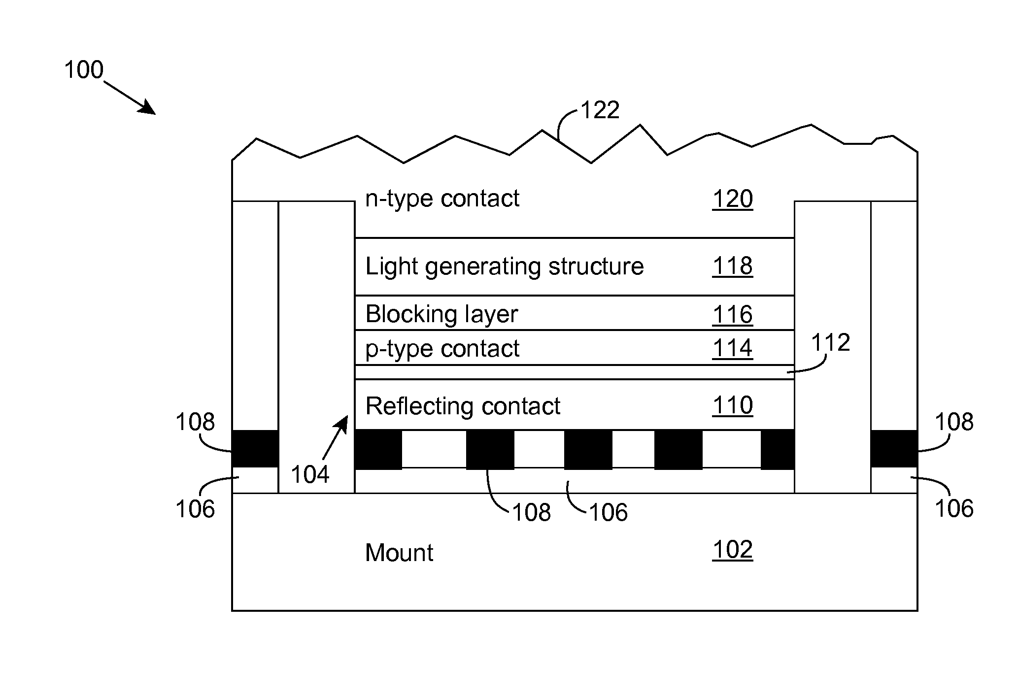
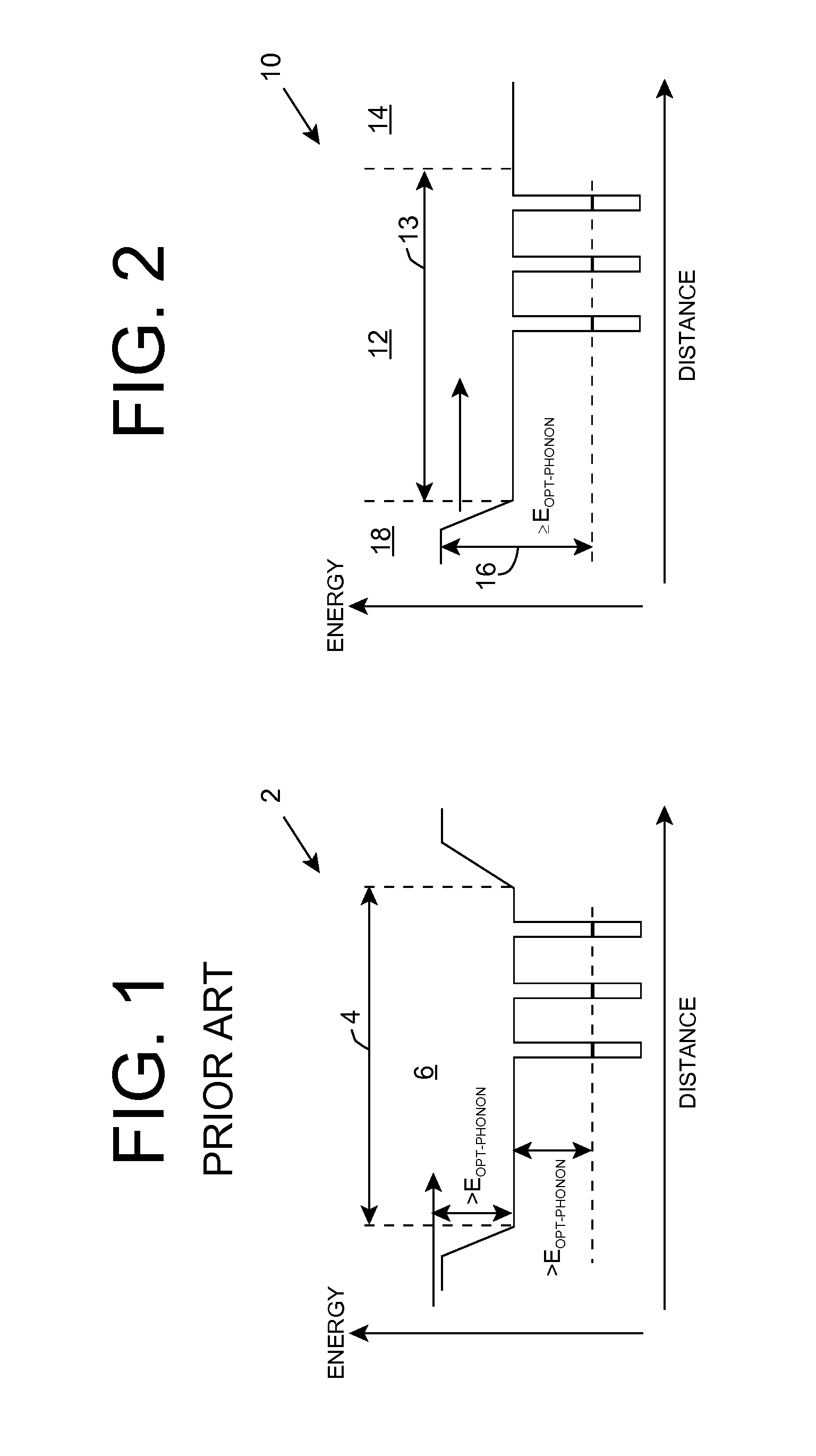
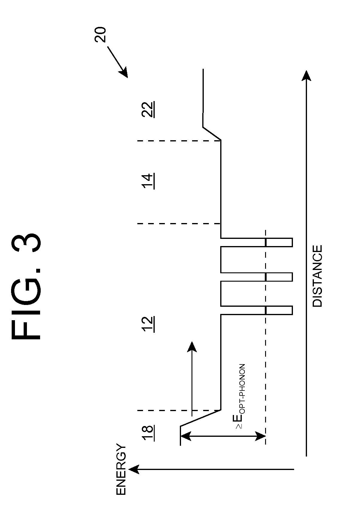
[0026]As indicated above, aspects of the invention provide a light emitting diode, which includes an n-type contact layer and a light generating structure adjacent to the n-type contact layer. The light generating structure includes a set of quantum wells. The contact layer and light generating structure can be configured so that a difference between an energy of the n-type contact layer and an electron ground state energy of a quantum well is greater than an energy of a polar optical phonon in a material of the light generating structure. Additionally, the light generating structure can be configured so that its width is comparable to a mean free path for emission of a polar optical phonon by an electron injected into the light generating structure. The diode can include a blocking layer, which is configured so that a difference between an energy of the blocking layer and the electron ground state energy of a quantum well is greater than the energy of the polar optical phonon in th...


PUM


Abstract

A light emitting diode is provided, which includes an n-type contact layer and a light generating structure adjacent to the n-type contact layer. The light generating structure includes a set of quantum wells. The contact layer and light generating structure can be configured so that a difference between an energy of the n-type contact layer and an electron ground state energy of a quantum well is greater than an energy of a polar optical phonon in a material of the light generating structure. Additionally, the light generating structure can be configured so that its width is comparable to a mean free path for emission of a polar optical phonon by an electron injected into the light generating structure. The diode can include a blocking layer, which is configured so that a difference between an energy of the blocking layer and the electron ground state energy of a quantum well is greater than the energy of the polar optical phonon in the material of the light generating structure. The diode can include a composite contact, including an adhesion layer, which is at least partially transparent to light generated by the light generating structure and a reflecting metal layer configured to reflect at least a portion of the light generated by the light generating structure.

Description

REFERENCE TO PRIOR APPLICATIONS[0001]The current application claims the benefit of co-pending U.S. Provisional Application No. 61 / 356,484, titled “Deep ultraviolet diode,” which was filed on 18 Jun. 2010, and which is hereby incorporated by reference.GOVERNMENT LICENSE RIGHTS[0002]The U.S. Government has a paid-up license in this invention and the right in limited circumstances to require the patent owner to license others on reasonable terms as provided for by the terms of SBIR Phase II Grant No. IIP-0956746 awarded by the National Science Foundation.TECHNICAL FIELD[0003]The disclosure relates generally to nitride-based heterostructures, and more particularly, to an improved ultraviolet light emitting nitride-based heterostructure.BACKGROUND ART[0004]Emerging deep ultraviolet light emitting diodes (DUV LEDs) cover the ultraviolet (UV) range down to 210 nanometers (nm), and provide output powers already sufficient for many applications. Additionally, these devices have high modulati...

Claims


Application Information

Patent Timeline
Patent Type & Authority Applications(United States)
IPC IPC(8): H01L33/06B82Y20/00
CPCH01L33/04H01L33/06H01L33/405H01L33/22H01L33/385H01L33/10H01L33/32
Inventor GASKA, REMIGIJUSSHATALOV, MAXIM S.SHUR, MICHAEL
Owner SENSOR ELECTRONICS TECH
Why Eureka
Try Eureka