Solar cell and method for fabricating the heterojunction thereof

a solar cell and heterojunction technology, applied in the field of high-efficiency solar cells, can solve the problems of limiting the power conversion efficiency (pce) of the polymer/silicon heterojunction solar cell, weak absorption, and limiting the power conversion efficiency (pce) of these cells to below 1%, so as to increase the exciton dissociation probability, improve the efficiency of solar cell production, and stabilize the behavior of the diod

Inactive Publication Date: 2011-12-29
NAT TAIWAN UNIV
View PDF12 Cites 19 Cited by
  • Summary
  • Abstract
  • Description
  • Claims
  • Application Information

AI Technical Summary

Benefits of technology

[0008]An object of this invention is to provide solar cells and method for producing their heterojunctions, as well as promoting the incident photo-to-current conversion efficiency (IPCE), and reducing the material and fabricating cost.
[0011]In an embodiment, the hole-conducting polymer poly(3,4-ethylenedioxythiophene):poly(styrenesulfonate) (PEDOT:PSS) is coated on the silicon nanowires (SiNWs) to replace the conventional p-doped amorphous or nanocrystal silicon layer and thus form a solar cell having SiNW / PEDOT heterojunctions. The highest occupied molecular orbital (HOMO) energy of PEDOT is about 5.1 eV, which is similar to the valence band energy of silicon. Thus, the interface between the PEDOT layer and n-type SiNWs could possibly form good heterojunctions for electron-hole pairs (EHPs) separation.
[0012]According to the embodiment, the current-to-voltage (J-V) characteristics of the SiNW / PEDOT solar cell clearly reveal a stable rectifying diode behavior. In addition, the heterojunctions can greatly increase the exciton dissociation probability and induce light trapping effect, leading to enhanced IPCE in the near infrared region. The power conversion efficiency (PCE) is also greatly improved as compared with the solar cells without nanowire / polymer heterojunctions.
[0013]According to an embodiment of this invention, a same semiconductor substrate can be repeatedly used to form nanostructures, greatly reducing the material cost. In addition, the fabricating steps may preferably use solution process to reduce the fabricating cost.

Problems solved by technology

This limits the power conversion efficiency (PCE) of the polymer / silicon heterojunction solar cells.
In addition, the nanowire structure significantly reduces the reflection and induces strong light trapping between nanowires, resulting in strong absorption.
High series and low shunt resistances appear to limit the power conversion efficiency (PCE) of these cells to below 1%.

Method used


Image

  • Solar cell and method for fabricating the heterojunction thereof
  • Solar cell and method for fabricating the heterojunction thereof
  • Solar cell and method for fabricating the heterojunction thereof

Examples


Embodiment Construction

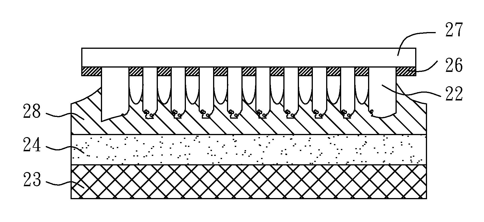
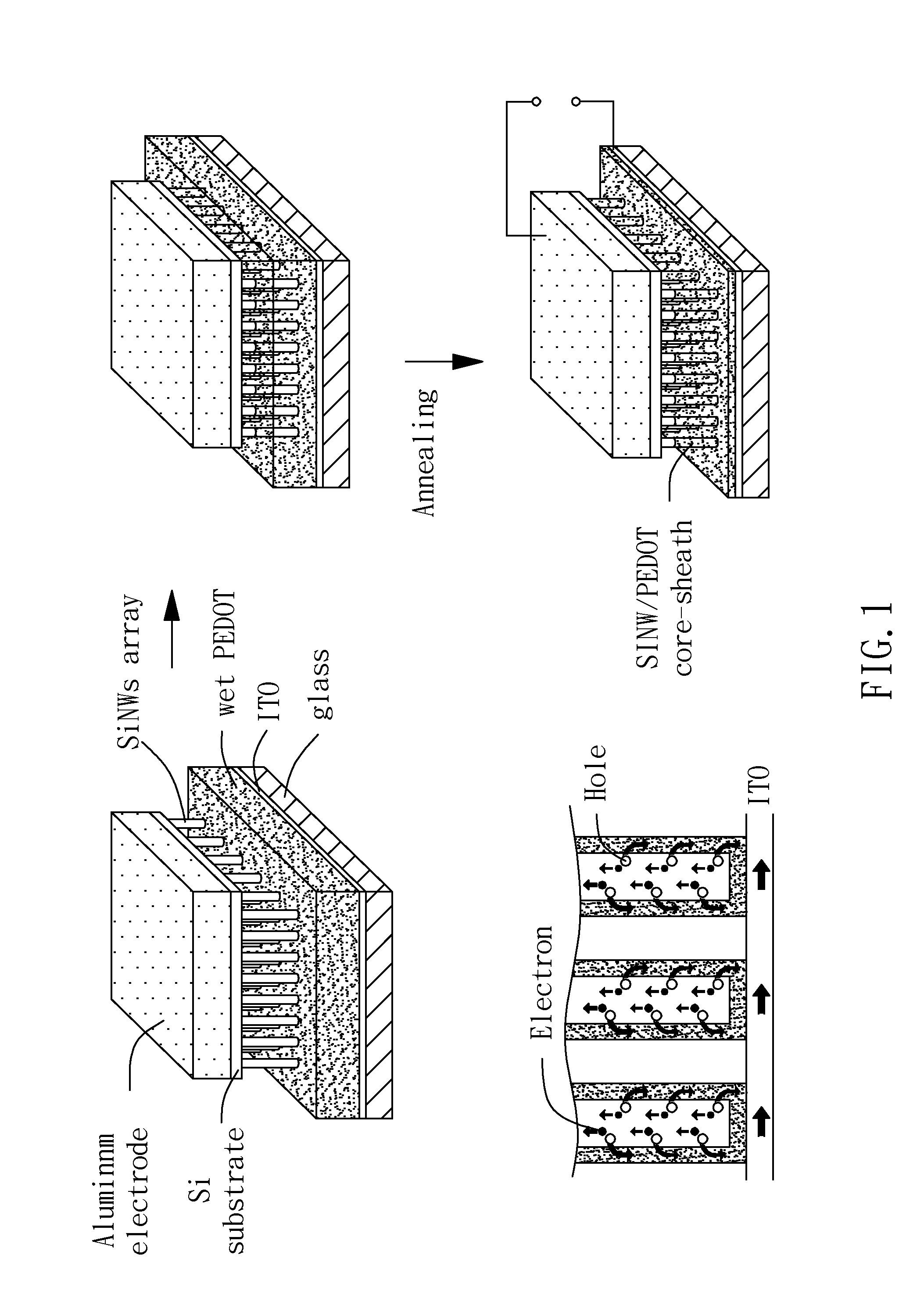
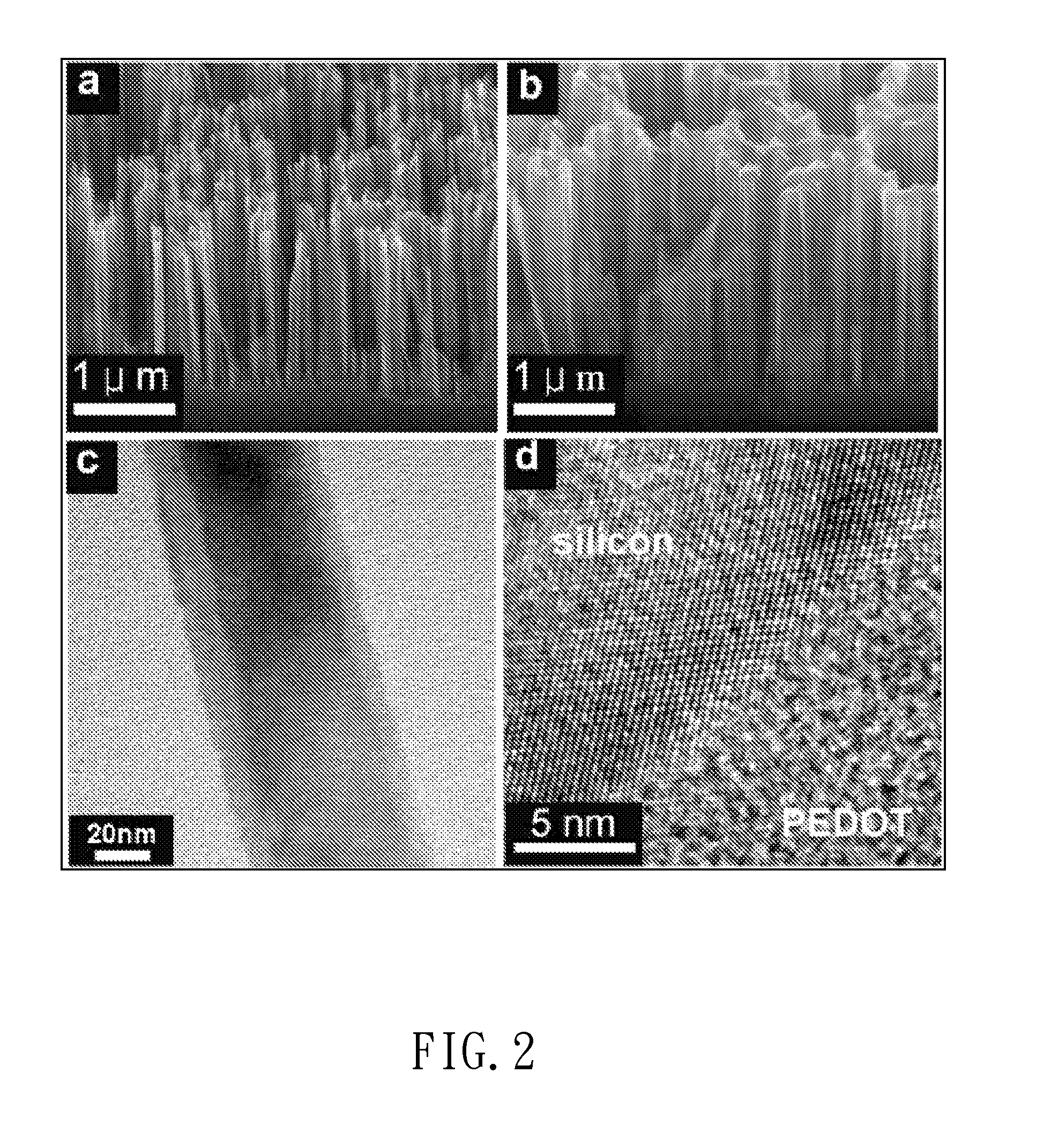
[0021]Reference will now be made in detail to specific embodiments of the invention. Examples of these embodiments are illustrated in accompanying drawings. While the invention will be described in conjunction with these specific embodiments, it will be understood that it is not intended to limit the invention to these embodiments. On the contrary, it is intended to cover alternatives, modifications, and equivalents as may be included within the spirit and scope of the invention as defined by the appended claims. In the following description, numerous specific details are set forth in order to provide a thorough understanding of the present invention. The present invention may be practiced without some or all of these specific details. In other instances, well-known process operations and components are not described in detail in order not to unnecessarily obscure the present invention. While drawings are illustrated in detail, it is appreciated that the quantity of the disclosed co...


PUM

PropertyMeasurementUnit
valence band energyaaaaaaaaaa
mean diameteraaaaaaaaaa
temperatureaaaaaaaaaa

Abstract

Embodiments of the present invention provide methods to fabricate semiconductor nanostructure / polymer heterojunctions of solar cells. The methods comprise that a conductive polymer is adhered on the surface of semiconductor nanostructures by capillary effect and core-sheath shaped heterojunctions are formed. The incident photo-to-current conversion efficiency (IPCE) of the solar cells having core-sheath heterojunctions can reach 30% or more.

Description

CROSS-REFERENCE TO RELATED APPLICATIONS[0001]The entire contents of Taiwan Patent Application No. 099120910, filed on Jun. 25, 2010, from which this application claims priority, are incorporated herein by reference.BACKGROUND OF THE INVENTION[0002]1. Field of the Invention[0003]The present invention generally relates to high efficiency solar cells and methods for fabricating their heterojunctions.[0004]2. Description of Related Art[0005]In the field of solar cell, the polymer / semiconductor heterojunction attracts lots of attention due to several advantages including free concern of lattice mismatch, large-area coverage, low-temperature process-capability, easy preparation, low cost, and so on. To date, researchers have demonstrated planar polymer / semiconductor heterojunction solar cells based on crystalline or amorphous silicon such as Poly-(CH3)3Si-Cyclooctatetraene / n-Si, tetraphenylporphyrin / n-Si, 4-tricyanovinyl-N,N-diethylaniline / p-Si, poly(3-hexylthiophene) / a-Si, poly(3,4-ethyl...

Claims


Application Information

Patent Timeline
Patent Type & Authority Applications(United States)
IPC IPC(8): H01L31/06H01L31/0352B82Y40/00
CPCB82Y20/00B82Y40/00H01L31/035227H01L31/03529Y02E10/549H01L51/0037H01L51/4213H01L51/4266H01L31/072H10K85/1135H10K30/10H10K30/352
Inventor LIN, CHING-FUHSYU, SHU-JIA
Owner NAT TAIWAN UNIV
Why Eureka
Try Eureka