Photoelectric conversion device, package structure therefor, and method of manufacturing photoelectric conversion device

a technology of photoelectric conversion and package structure, which is applied in the direction of electrical equipment, semiconductor devices, radio frequency controlled devices, etc., can solve the problems of poor light-blocking properties of glass chips b>132/b>, large number of steps, and low yield, so as to reduce size (tallness, thickness) and cost, and improve light-blocking properties. , the effect of simple structur

Inactive Publication Date: 2011-12-29
SONY SEMICON SOLUTIONS CORP
View PDF2 Cites 30 Cited by
  • Summary
  • Abstract
  • Description
  • Claims
  • Application Information

AI Technical Summary

Benefits of technology

[0039]In accordance with the one embodiment of the present technology, a method of manufacturing a photoelectric conversion device includes: a first step of forming a plurality of photoelectric conversion regions on a surface on one side of a semiconductor wafer; a second step of preparing a light-blocking wafer having insertion openings each formed so that an optical element is inserted therein from at least one side, the insertion openings corresponding respectively to the photoelectric conversion regions; a third step of bonding the one-side surface of the semiconductor wafer and a surface on the opposite side to a surface on the one side of the light-blocking wafer to each other, in such a manner that the photoelectric conversion regions and the insertion openings correspond to each other, to form a bonded wafer body; and a fourth step of dividing the bonded wafer body in peripheries of the photoelectric conversion regions, to obtain bonded-body chips each having the photoelectric conversion region. Therefore, by utilizing the wafer level chip size packaging (WLCSP) process, it is possible to provide a method of manufacturing a photoelectric conversion device wherein a simple structure and an excellent light-blocking property are ensured and reductions in size (tallness, thickness) and cost can be realized.
[0040]Besides, in accordance with the another embodiment of the present technology, in regard to a semiconductor wafer having a plurality of

Problems solved by technology

This method, however, is disadvantageous in that a troublesome work of bonding tiny chips (the bonded-body chip and the lens chip 152) to each other is included in the method and that the number of steps is large.
This method, therefore, is

Method used


Image

  • Photoelectric conversion device, package structure therefor, and method of manufacturing photoelectric conversion device
  • Photoelectric conversion device, package structure therefor, and method of manufacturing photoelectric conversion device
  • Photoelectric conversion device, package structure therefor, and method of manufacturing photoelectric conversion device

Examples


embodiments

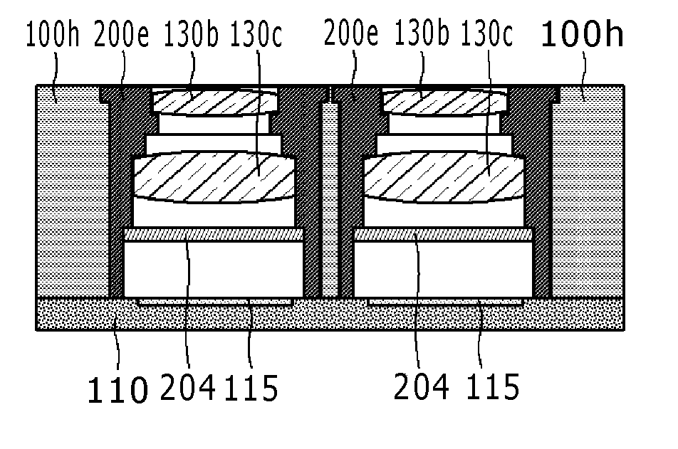
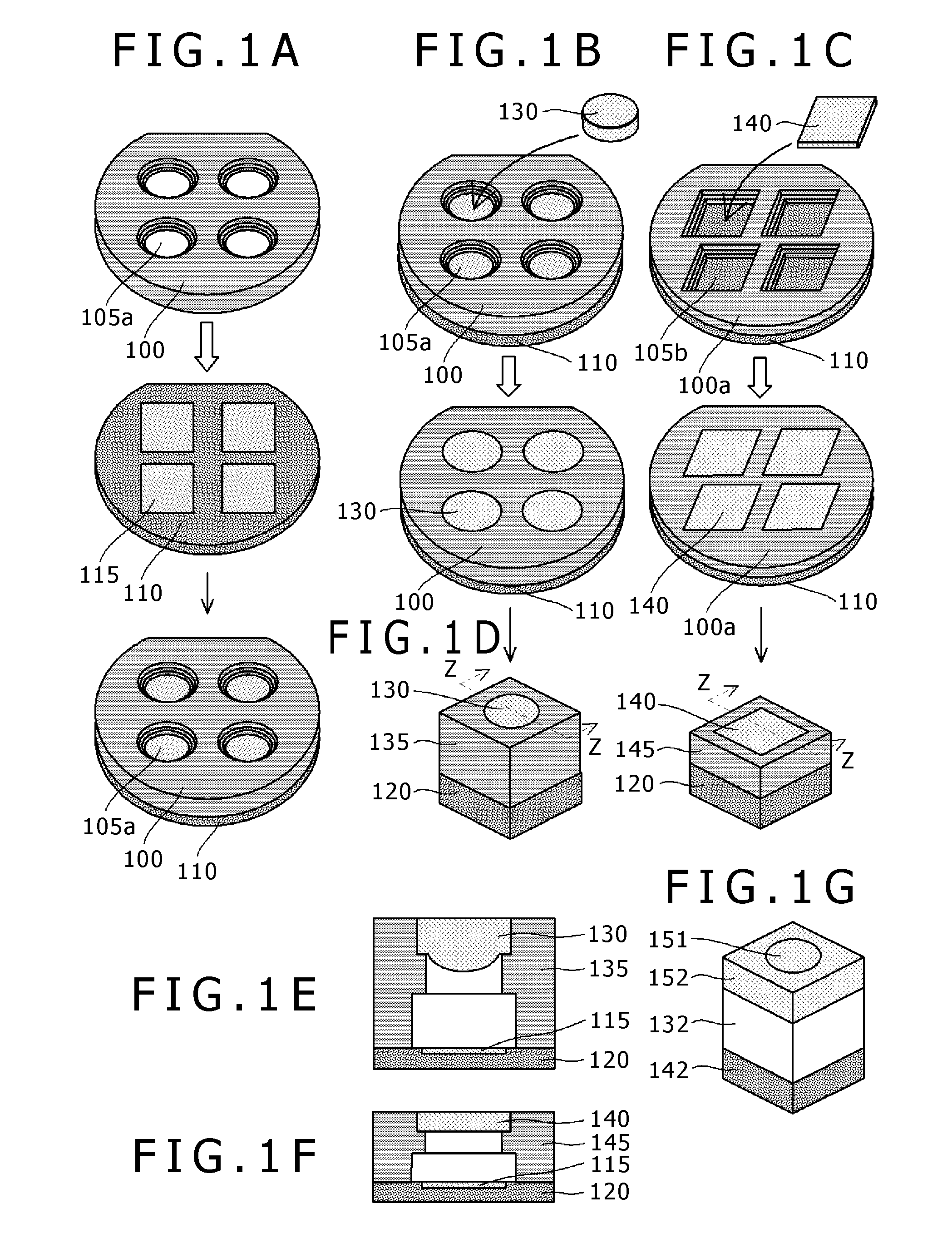
[0084]FIGS. 1A to 1F illustrate methods of manufacturing a camera module and configurations of the camera modules, in embodiments of the present technology, wherein FIG. 1A shows perspective views for illustrating bonding between a black wafer and a semiconductor wafer, FIGS. 1B and 1C show perspective views for illustrating insertion of optical elements into insertion openings formed in a black wafer, FIG. 1D shows perspective views for each illustrating a module obtained by cutting a bonded wafer body into individual pieces, and FIGS. 1E and 1F show ZZ sectional views of the modules, with FIG. 1G being a perspective view for illustrating a camera module according to related art.

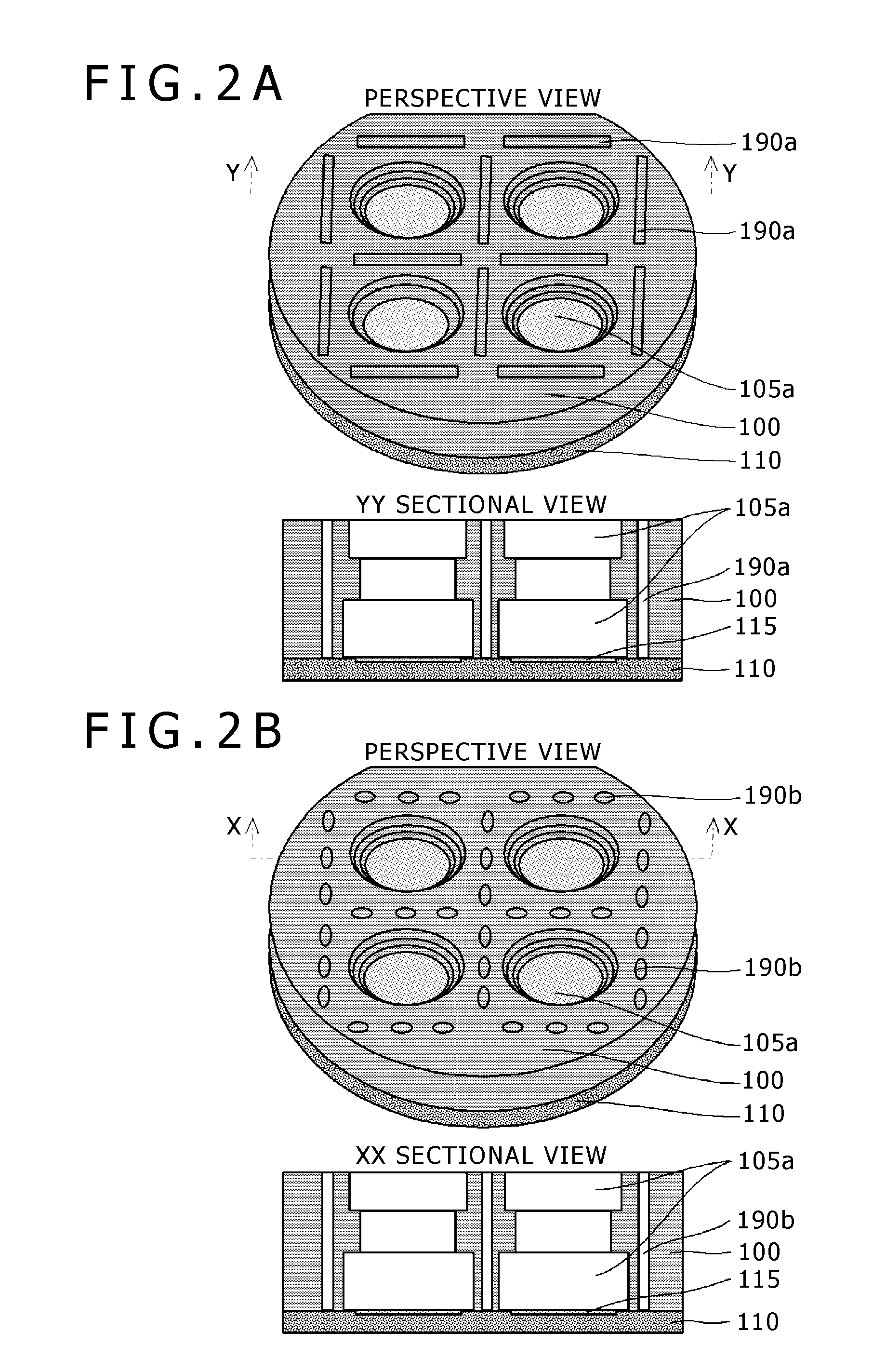
[0085]As shown in FIG. 1A, a black wafer 100 having a plurality of insertion openings 105a formed so that optical elements such as lenses 130, etc. or optical barrels described later are to be inserted and fixed therein and a semiconductor wafer 110 formed with a plurality of image sensor regions 115 are bo...


PUM


Abstract

The present disclosure provides a method of manufacturing a photoelectric conversion device, including, a first step of forming a plurality of photoelectric conversion regions on a surface on one side of a semiconductor wafer, a second step of preparing a light-blocking wafer having insertion openings, a third step of bonding the one-side surface of the semiconductor wafer and a surface on the opposite side to a surface on the one side of the light-blocking wafer to each other to form a bonded wafer body, and a fourth step of dividing the bonded wafer body in peripheries of the photoelectric conversion regions, to obtain bonded-body chips each having the photoelectric conversion region.

Description

BACKGROUND[0001]The present technology relates to a photoelectric conversion device, a package structure therefor, and a method of manufacturing a photoelectric conversion device wherein a simple structure and an excellent light blocking-property are ensured and reductions in size (tallness, thickness) and cost can be realized.[0002]Mobile apparatuses such as cell phones, PDAs (personal digital assistance), notebook type computers, etc. on which a small-sized camera module including an optical part such as a lens, etc. and a solid state imaging element is mounted have come to be used widely. With respect to the camera modules mounted on these mobile apparatuses, further reductions in size (tallness, thickness) and in cost are being demanded.[0003]Normally, the camera module includes an image sensor chip formed with a solid state imaging element such as CCD (Charge Coupled Device), CMOS (Complementary Metal-Oxide Semiconductor), etc. and an imaging lens (optical lens) for forming a s...

Claims


Application Information

Patent Timeline
IPC IPC(8): H01L31/02
CPCH01L27/14618H01L27/14683H01L27/14623H01L2924/0002H01L2924/00
Inventor NIHEI, YASUHIDE
Owner SONY SEMICON SOLUTIONS CORP
Why Eureka
Try Eureka