Liquid crystal display device and electronic appliance
- Summary
- Abstract
- Description
- Claims
- Application Information
AI Technical Summary
Benefits of technology
Problems solved by technology
Method used
Image

Examples
embodiment 1
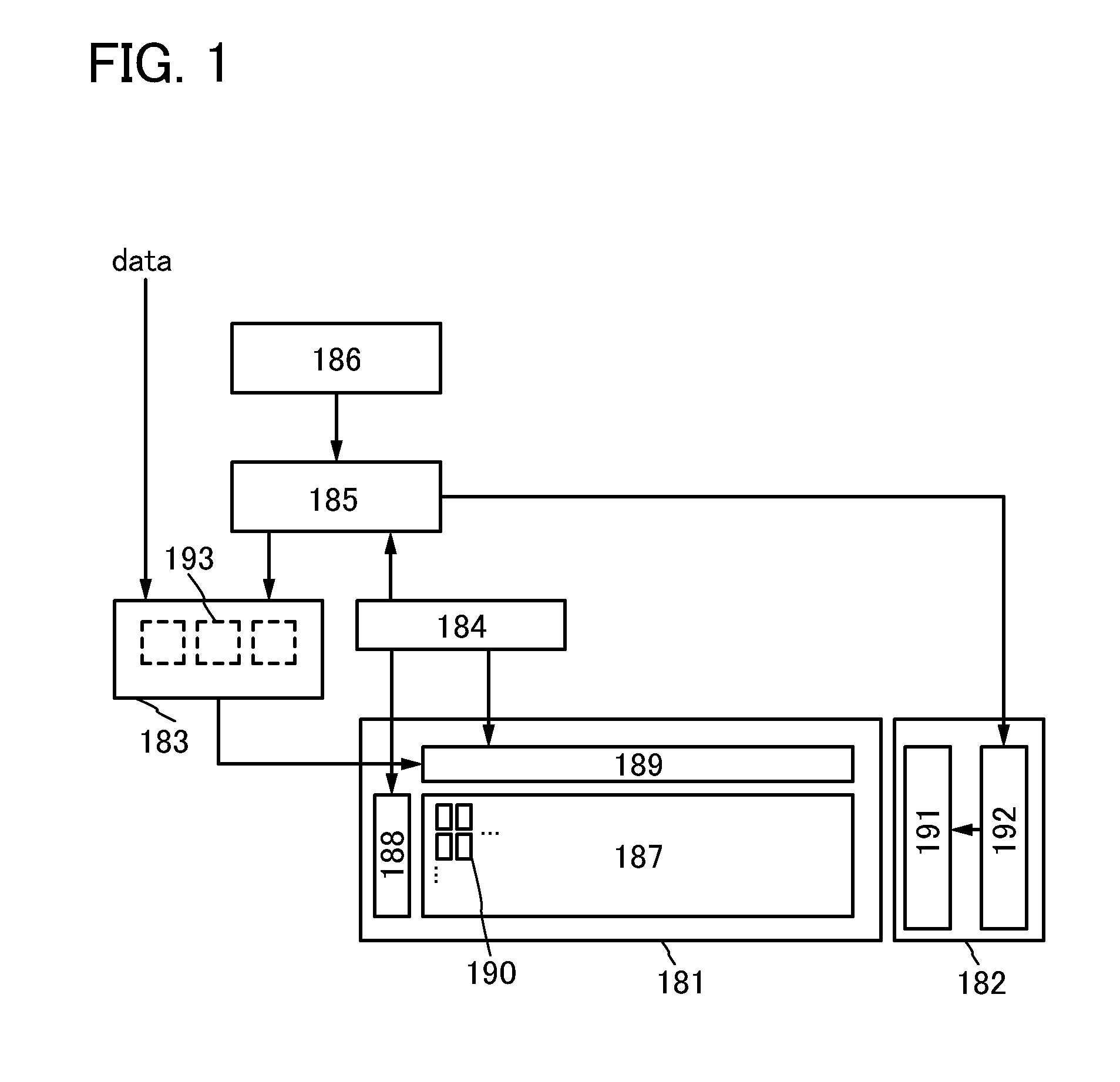
[0042]First, FIG. 1 is a block diagram illustrating a liquid crystal display device. The liquid crystal display device in FIG. 1 includes a display panel 181, a backlight portion 182, a video signal selection circuit 183, a control circuit 184, a sequence determination circuit 185, and a random number generation circuit 186.
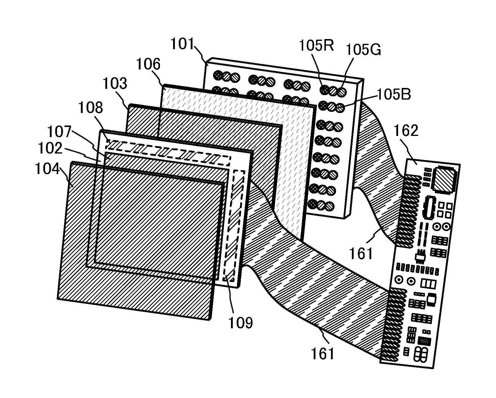
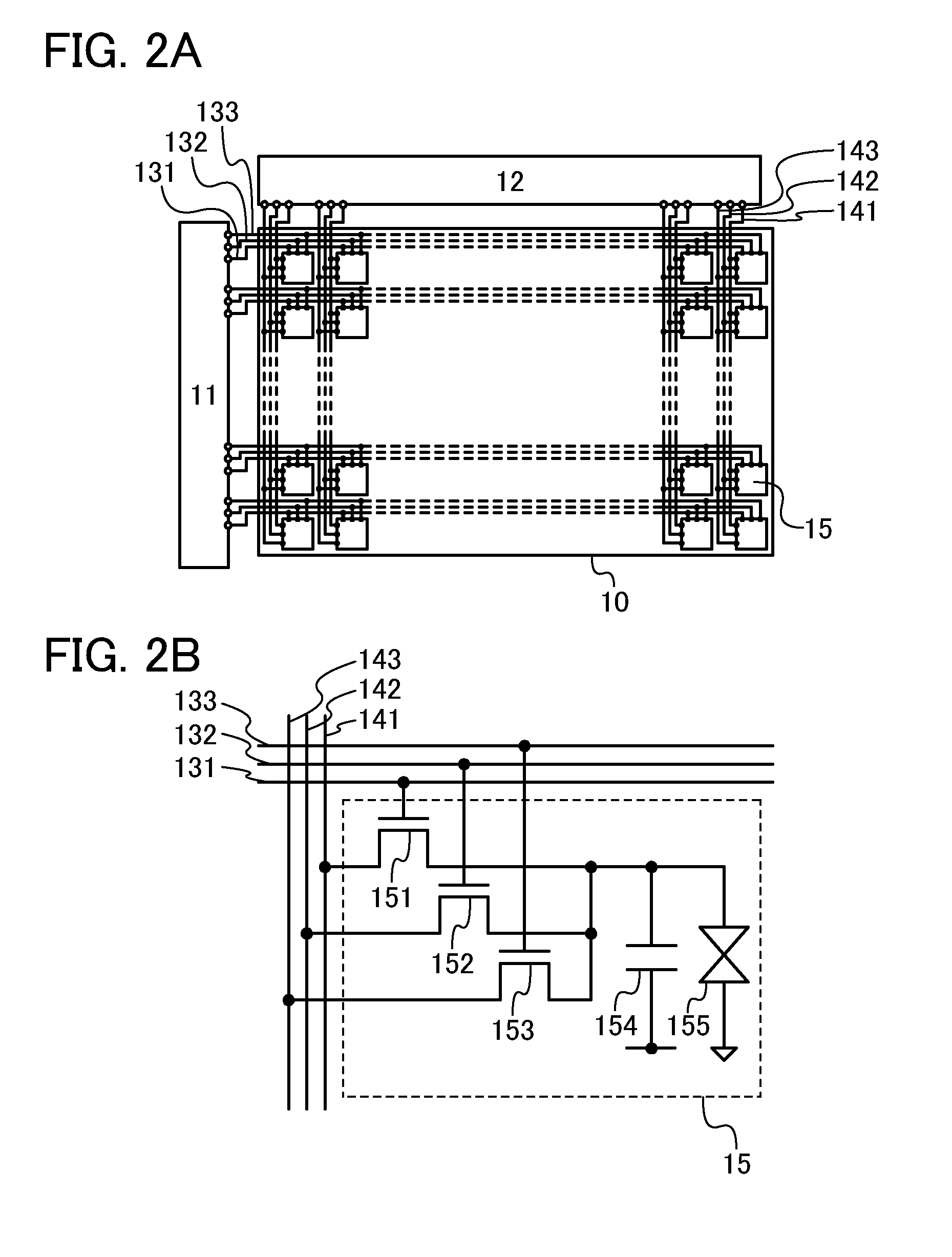
[0043]The display panel 181 includes a pixel portion 187, a scan line driver circuit 188, and a signal line driver circuit 189. The pixel portion 187 includes a plurality of pixels 190. Each of the pixels 190 includes a transistor serving as a circuit portion that selects a pixel, a pixel electrode connected to the transistor, and a capacitor. Note that a liquid crystal element is formed in such a manner that a liquid crystal layer is sandwiched between the pixel electrode and an electrode paired with the pixel electrode. To the scan line driver circuit 188 and the signal line driver circuit 189, control signals for operating the driver circuits (e.g., a clock si...
embodiment 2
[0120]In this embodiment, a structure where there are periods in each of which light sources of a backlight do not emit light before and after a period that is one frame period will be described, which is different from the structure in FIG. 6 described in Embodiment 1 showing scanning of selection signals and timings of light emission of the light sources in the backlight. Note that common description between Embodiment 1 and this embodiment will be omitted in this embodiment.
[0121]FIG. 9 is a timing chart showing scanning of selection signals and timings of light emission of light sources in a backlight in the case where there are periods in each of which the light sources of the backlight do not emit light before and after a period that is one frame period. The length of the period in which the light sources in the backlight do not emit light is not particularly limited as long as display quality is not degraded.
[0122]In the timing chart in FIG. 9, as in FIG. 6, in the sampling p...
embodiment 3
[0133]In this embodiment, examples of a transistor that can be applied to a liquid crystal display device disclosed in this specification will be described. There is no particular limitation on the structure of the transistor that can be applied to the liquid crystal display device disclosed in this specification. For example, a staggered transistor, a planar transistor, or the like having a top-gate structure in which a gate electrode is placed over a semiconductor layer with a gate insulating layer provided therebetween or a bottom-gate structure in which a gate electrode is placed below a semiconductor layer with a gate insulating layer provided therebetween, can be used. Further, the transistor may have a single gate structure including one channel formation region, a double gate structure including two channel formation regions, or a triple gate structure including three channel formation regions. Alternatively, the transistor may have a dual gate structure including two gate e...
PUM
 Abstract
Description
Claims
Application Information
 - R&D
- Intellectual Property
- Life Sciences
- Materials
- Tech Scout
- Unparalleled Data Quality
- Higher Quality Content
- 60% Fewer Hallucinations
Browse by: Latest US Patents, China's latest patents, Technical Efficacy Thesaurus, Application Domain, Technology Topic, Popular Technical Reports.
© 2025 PatSnap. All rights reserved.Legal|Privacy policy|Modern Slavery Act Transparency Statement|Sitemap|About US| Contact US: help@patsnap.com